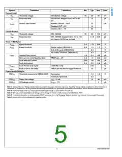
Symbol
Current Limit
VCL
Parameter
Threshold voltage
Conditions
VIN-SENSE voltage
Min.
45
Typ. Max. Units
50
15
55
mV
µs
tCL
Response time
VIN-SENSE stepped from 0 mV to 80
mV
ISENSE
SENSE input current
Enabled, SENSE = OUT
Disabled, OUT = 0V
Enabled, OUT = 0V
23
12
62
µA
Circuit Breaker
VCB
tCB
Threshold voltage
Response time
VIN - SENSE
75
95
110
mV
µs
VIN - SENSE stepped from 0 mV to 150
mV, time to GATE low, no load
0.19
0.36
Timer (TIMER pin)
VTMRH Upper threshold
VTMRL
1.6
0.9
1.72
1.0
0.3
0.3
-5.5
2
1.85
1.1
V
V
Lower threshold
Restart cycles (LM25069-2)
End of 8th cycle (LM25069-2)
Re-enable Threshold (LM25069-1)
V
V
ITIMER
Insertion time current
-7.5
1.5
-3.5
2.5
-50
3.4
µA
mA
µA
µA
%
Sink current, end of insertion time
Fault detection current
Fault sink current
TIMER pin = 2V
-110
1.6
-80
2.5
0.67
20
DCFAULT
tFAULT
Fault Restart Duty Cycle
Fault to GATE low delay
LM25069-2 only
TIMER pin reaches the upper threshold
µs
Power Good (PGD pin)
PGDTH
Threshold measured at SENSE-OUT
Decreasing
1.3
0.6
15
1.9
V
Threshold Hysteresis
ISINK = 2 mA
PGDVOL
PGDIOH
Output low voltage
Off leakage current
30
1
mV
µA
VPGD = 17V
Note 1: Absolute Maximum Ratings indicate limits beyond which damage to the device may occur. Operating Ratings indicate conditions for which the device is
intended to be functional, but do not guarantee specific performance limits. For guaranteed specifications and conditions see the Electrical Characteristics.
Note 2: The human body model is a 100 pF capacitor discharged through a 1.5 kΩ resistor into each pin.
Note 3: OUT bias current (disabled) due to leakage current through an internal 1.0 MΩ resistance from SENSE to VOUT.
Note 4: For detailed information on soldering plastic MSOP packages refer to the Packaging Databook available from National Semiconductor Corporation.
Note 5: Current out of a pin is indicated as a negative number.
5
www.national.com

 NSC [ National Semiconductor ]