Storage Temperature
Junction Temperature
Lead Temperature (soldering 4 sec)
-65°C to +150°C
+150°C
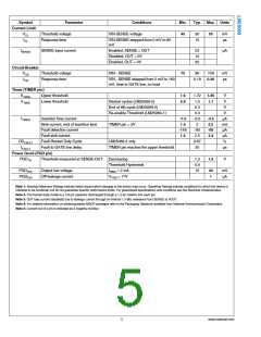
Absolute Maximum Ratings (Note 1)
If Military/Aerospace specified devices are required,
please contact the National Semiconductor Sales Office/
Distributors for availability and specifications.
+260°C
Operating Ratings
VIN Supply Voltage
VIN to GND (Note 5)
SENSE, OUT, PGD to GND
UVLO to GND
OVLO to GND
VIN to SENSE
-0.3V to 20V
-0.3V to 20V
-0.3V to 20V
-0.3V to 20V
-0.3V to +0.3V
2kV
+2.9V to 17V
PGD Off Voltage
0V to 17V
Junction Temp. Range
−40°C to +85°C
ESD Rating (Note 2)
Human Body Model
Electrical Characteristics Limits in standard type are for TJ = 25°C only; limits in boldface type apply over the
junction temperature (TJ) range of -40°C to +85°C. Minimum and Maximum limits are guaranteed through test, design, or statistical
correlation. Typical values represent the most likely parametric norm at TJ = 25°C, and are provided for reference purposes only.
Unless otherwise stated the following conditions apply: VIN = 12V.
Symbol
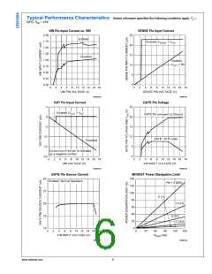
Input (VIN pin)
IIN-EN
Parameter
Conditions
Min.
Typ. Max. Units
Input Current, enabled
Input Current, disabled
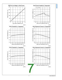
Power On Reset threshold at VIN
POR hysteresis
UVLO = 2V and OVLO = 0.7V, VIN = 14V
UVLO = 0.7V or OVLO = 2V
VIN Increasing
1.6
1.0
2.6
150
2.4
1.6
2.8
mA
mA
V
IIN-DIS
POR
PORHYS
OUT pin
IOUT-EN
VIN decreasing
mV
OUT bias current, enabled
OUT = VIN, Normal operation
0.30
-12
µA
IOUT-DIS
OUT bias current, disabled (Note 3)
Disabled, OUT = 0V, SENSE = VIN
UVLO, OVLO pins
UVLOTH
UVLOHYS
UVLODEL
UVLO threshold
1.154
15
1.17 1.183
V
UVLO hysteresis current
UVLO delay
UVLO = 1V
20
15
26
µA
µs
Delay to GATE high
Delay to GATE low
UVLO = 3V
8.3
UVLOBIAS
OVLOTH
UVLO bias current
OVLO threshold
1
µA
V
1.142
-26
1.16 1.185
OVLOHYS
OVLODEL
OVLO hysteresis current
OVLO delay
OVLO = 2V
-20
16
-15
µA
µs
Delay to GATE high
Delay to GATE low
OVLO = 1V
8.2
OVLOBIAS
OVLO bias current
1
µA
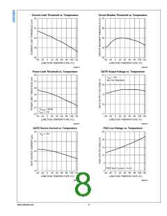
Power Limit (PWR pin)
PWRLIM-1
PWRLIM-2
IPWR
Power limit sense voltage (VIN-SENSE)
19
19
25
25
31
31
mV
mV
µA
Ω
SENSE-OUT = 12V, RPWR = 69.8 kΩ
SENSE-OUT = 6V, RPWR = 34.8 kΩ
VPWR = 2.5V
PWR pin current
-15
140
RSAT(PWR)
PWR pin impedance when disabled
UVLO = 0.7V
Gate Control (GATE pin)
IGATE
Source current
Sink current
Normal Operation
UVLO = 1V
-27
1.5
-20
2
-13
2.5
µA
mA
mA
VIN - SENSE = 150 mV or VIN < POR,
VGATE = 5V
160
260
375
VGATE
Gate output voltage in normal operation GATE voltage with respect to ground
18
19.5
20.5
V
www.national.com
4

 NSC [ National Semiconductor ]