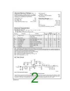
routing and component placement from pin 1 of the LM2435
to the red cathode. Note that the components are placed so
that they almost line up from the output pin of the LM2435 to
the red cathode pin of the CRT connector. This is done to
minimize the length of the video path between these two
components. Note also that the arc protection diodes, D16
and D17 are placed close to L1 and C14 in order to minimize
the size of the node connecting all these components. R21
and D9 are placed close to C14 and R32 for the same rea-
son. This minimizes parasitic capacitance in the video path
and also enhances the effectiveness of the protection di-
odes. The anode of protection diode D16 is connected di-
rectly to a section of the ground plane that has a short and
direct path to the LM2435 ground. The cathode of D16 is
connected to VCC very close to decoupling capacitor C53
(see Figure 12) which is connected to the same section of
the ground plane as D17. The diode placement and routing
is very important for minimizing the voltage stress on the
LM2435 during an arc over event. Lastly, notice that S1 is
placed very close to the red cathode and is tied directly to
CRT ground.
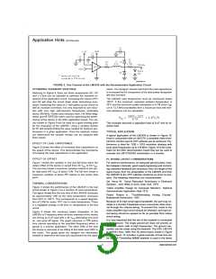
Application Hints (Continued)
board. Note that the heatsink is attached (soldered) to PCB
ground just to the left and just to the right of the device. The
LM2435 is attached to the heatsink using a screw, star
washer and nut. The star washer should be located on the
side of the heatsink opposite the device.
NSC DEMONSTRATION BOARD
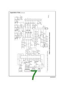
Figure 11 shows routing and component placement on the
NSC LM1279/243X demonstration board. The schematic of
the board is shown in Figure 10. This board provides a good
example of a layout that can be used as a guide for future
layouts. Note the location of the following components:
•
•
•
C54, C56 — VCC bypass capacitor, located very close to
pin 4 and ground connections to the device.
C43, C44 — VBB bypass capacitors, located close to pin
8 and ground.
C53, C55 — VCC bypass capacitors, near LM2435 and
VCC clamp diodes. This is very important for arc protec-
tion.
The routing of the LM2435 outputs to the CRT is very critical
to achieving optimum performance. Figure 12 shows the
www.national.com
6

 NSC [ National Semiconductor ]