device to PCB ground is very important. It is critical that the
device tab is connected to PCB Ground through the heat-
sink, in order to eliminate excessive overshoot and ringing.
The LM1279/243X (Rev. B) demo board provides a good ex-
ample of how to do this.
Theory of Operation
The LM2435 is a high voltage monolithic three channel CRT
driver suitable for high resolution display applications. The
LM2435 operates with 80V and 12V power supplies. The
part is housed in the industry standard 9-lead TO-220
molded plastic power package.
POWER SUPPLY BYPASS
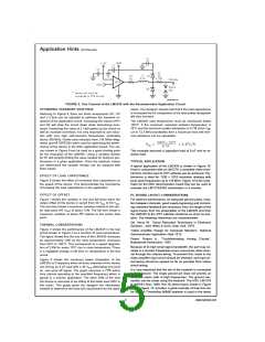
The circuit diagram of the LM2435 is shown in Figure 1. The
PNP emitter follower, Q5, provides input buffering. Q1 and
Q2 form a fixed gain cascode amplifier with resistors R1 and
R2 setting the gain at −14. Emitter followers Q3 and Q4 iso-
late the high output impedance of the cascode stage from
the capacitance of the CRT cathode which decreases the
sensitivity of the device to load capacitance. Q6 provides bi-
asing to the output emitter follower stage to reduce cross-
over distortion at low signal levels.
Since the LM2435 is a wide bandwidth amplifier, proper
power supply bypassing is critical for optimum performance.
Improper power supply bypassing can result in large over-
shoot, ringing or oscillation. A 0.1 µF capacitor should be
connected from the supply pin, VCC, to ground, as close to
the supply and ground pins as is practical. Additionally, a
10 µF to 100 µF electrolytic capacitor should be connected
from the supply pin to ground. The electrolytic capacitor
should also be placed reasonably close to the LM2435’s
supply and ground pins. A 0.1 µF capacitor should be con-
nected from the bias pin, VBB, to ground, as close as is prac-
tical to the part.
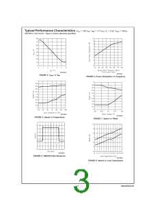
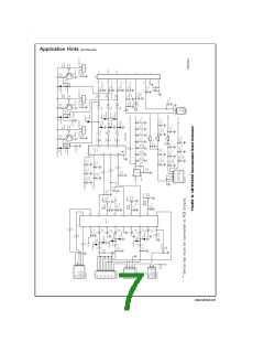
Figure 2 shows a typical test circuit for evaluation of the
LM2435. This circuit is designed to allow testing of the
LM2435 in a 50Ω environment without the use of an expen-
sive FET probe. In this test circuit, two low inductance resis-
tors in series totaling 4.98 kΩ form a 200:1 wideband, low
capacitance probe when connected to a 50Ω coaxial cable
and a 50Ω load (such as a 50Ω oscilloscope input). The in-
put signal from the generator is ac coupled to the base of
Q5.
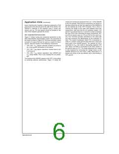
ARC PROTECTION
During normal CRT operation, internal arcing may occasion-
ally occur. Spark gaps, in the range of 200V, connected from
the CRT cathodes to CRT ground will limit the maximum volt-
age, but to a value that is much higher than allowable on the
LM2435. This fast, high voltage, high energy pulse can dam-
age the LM2435 output stage. The application circuit shown
in Figure 9 is designed to help clamp the voltage at the out-
put of the LM2435 to a safe level. The clamp diodes, D1 and
D2, should have a fast transient response, high peak current
rating, low series impedance and low shunt capacitance.
FDH400 or equivalent diodes are recommended. Do not use
1N4148 diodes for the clamp diodes. D1 and D2 should have
short, low impedance connections to VCC and ground re-
spectively. The cathode of D1 should be located very close
to a separately decoupled bypass capacitor (C3 in Figure 9).
The ground connection of D2 and the decoupling capacitor
should be very close to the LM2435 ground. This will signifi-
cantly reduce the high frequency voltage transients that the
LM2435 would be subjected to during an arcover condition.
Resistor R2 limits the arcover current that is seen by the di-
odes while R1 limits the current into the LM2435 as well as
the voltage stress at the outputs of the device. R2 should be
a 1/2W solid carbon type resistor. R1 can be a 1/4W metal or
carbon film type resistor. Having large value resistors for R1
and R2 would be desirable, but this has the effect of increas-
ing rise and fall times. Inductor L1 is critical to reduce the ini-
tial high frequency voltage levels that the LM2435 would be
subjected to. The inductor will not only help protect the de-
vice but it will also help minimize rise and fall times as well as
minimize EMI. For proper arc protection, it is important to not
omit any of the arc protection components shown in Figure
9.
Application Hints
INTRODUCTION
National Semiconductor (NSC) is committed to provide ap-
plication information that assists our customers in obtaining
the best performance possible from our products. The follow-
ing information is provided in order to support this commit-
ment. The reader should be aware that the optimization of
performance was done using a specific printed circuit board
designed at NSC. Variations in performance can be realized
due to physical changes in the printed circuit board and the
application. Therefore, the designer should know that com-
ponent value changes may be required in order to optimize
performance in a given application. The values shown in this
document can be used as a starting point for evaluation pur-
poses. When working with high bandwidth circuits, good lay-
out practices are also critical to achieving maximum perfor-
mance.
IMPORTANT INFORMATION
The LM2435 performance is targeted for the SXGA (1280 x
1024, 75 Hz refresh) resolution market. The application cir-
cuits shown in this document to optimize performance and to
protect against damage from CRT arc-over are designed
specifically for the LM2435. If another member of the
LM243X family is used, please refer to its datasheet. Since
the LM2435 is a high speed amplifier, the connection of the
www.national.com
4

 NSC [ National Semiconductor ]