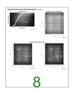
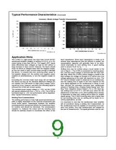
Application Hints (Continued)
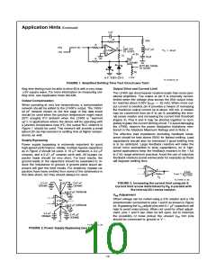
s
ꢁC
L
49 pF
TLꢀHꢀ9414–21
FIGURE 1ꢃ Simplified Settling Time Test Circuit (see Text)
tling time testing must be able to drive 50X with a very clean Output Drive and Current Limit
g
5V square waveꢁ For more information on measuring set-
tling timeꢂ see Application Note AN-428ꢁ
The LF400 can drive heavier resistive loads than most oper-
ational amplifiersꢁ The output at pin 6 is internally current-
limited when the voltage drop across the 25X output resis-
Output Compensation
e
tor reaches about 0ꢁ55V (I
22 mA)ꢁ When more out-
OUT
When operating at very low temperaturesꢂ a compensation
network should be added to the LF400’s outputꢁ The 100Xꢀ
22 pF network shown on the first page of this data sheet
should be used when the junction temperature might reach
25 C (roughly 0 C ambient when the LF400 is ‘‘warmed
put current is neededꢂ pin 8 provides a means of increasing
the maximum output current up to about 100 mAꢁ A resistor
may be connected from pin 8 to pin 6ꢂ paralleling the inter-
nal sense resistor and increasing the current limit threshold
(Figure 3)ꢁ Pins 6 and 8 may be shorted together to com-
pletely bypass the current limiting circuitꢁ To avoid damaging
the LF400ꢂ observe the power dissipation limitations men-
tioned in the Absolute Maximum Ratings and in Note 4ꢁ
ꢀ
ꢀ
up’’)ꢁ In applications where the device will be operating with
a junction temperature near 0 Cꢂ the output RLC network in
ꢀ
Figure 1 should be usedꢁ This network will provide a small
(about 20 ns) improvement in settling time at higher temper-
aturesꢂ as wellꢁ
The effective load impedance (including feedback resist-
ance) should be kept above 500X for fastest settlingꢁ Load
capacitance should also be minimized if good settling time
is to be optimizedꢁ Large feedback resistors will make the
circuit more susceptible to stray capacitanceꢂ so in high-
speed applications keep the feedback resistors in the 1 kX
to 2 kX range wherever practicalꢁ Avoid the use of inductive
feedback resistors (some wirewounds for example) as these
will degrade settling timeꢁ
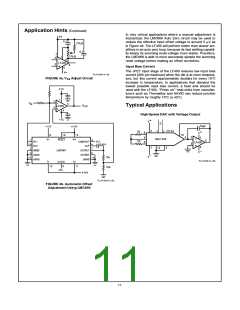
Supply Bypassing
Power supply bypassing is extremely important for good
high-speed performanceꢁ Ideallyꢂ multiple bypass capacitors
as in Figure 2 should be usedꢁ A 10 mF tantalumꢂ a 2ꢁ2 mF
ceramicꢂ and a 0ꢁ47 mF ceramic work wellꢁ All bypass ca-
pacitor leads should be very shortꢁ For best resultsꢂ the
ground leads of the capacitors should be separated to re-
duce the inductance to groundꢁ A ground plane layout ap-
proach will give the best resultsꢁ For simplicityꢂ bypass ca-
pacitors have been omitted from some of the schematics in
this data sheetꢂ but they should always be usedꢁ
0ꢁ55V
ꢀ
I
Limit
R ꢀꢀ25X
x
TLꢀHꢀ9414–23
FIGURE 3ꢃ Increasing the current limit using pin 8ꢃ
Current limit is now determined by R in parallel with
X
the internal 25X sense resistorꢃ
V
Adjustment
os
Offset voltage can be nulled using a 27k resistor and a 10k
potentiometer connected to pins 1 and 5 as shown inFigure
4aꢁ Bypassing the V adjust pins with 0ꢁ1 mF capacitors will
os
help to avoid noise pickupꢁ When not used for offset adjust-
mentꢂ pins 1 and 5 can often be left openꢂ but to minimize
the possibility of noise pickup the unused V trim pins
os
should be connected to ground or Vb
ꢁ
TLꢀHꢀ9414–22
FIGURE 2ꢃ Power Supply Bypassing (see Text)
10

 NSC [ National Semiconductor ]