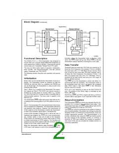
Deserializer Switching Characteristics
Over recommended operating supply and temperature ranges unless otherwise specified.
Symbol
Parameter
Conditions
Pin/Freq.
Min
Typ
Max
Units
tRCP
Receiver out Clock
Period
Figure 3
tRCP = tTCP
RCLK
25
62.5
ns
tCLH
tCHL
CMOS/TTL Low-to-High
Transition Time
CL = 15 pF
Figure 2
Rout(0-9),
2
2
6
6
ns
CMOS/TTL High-to-Low
Transition Time
LOCK, RCLK
ns
ns
ns
tDD
Deserializer Delay
Figure 4
Figure 5
1.75*tRCP+ 1.5 1.75*tRCP+4.0 1.75*tRCP+6.5
tROS
ROUT (0-9) Setup Data to
RCLK
RCLK
0.4*tRCP
0.5*tRCP
tROH
ROUT (0-9) Hold Data to
RCLK
−0.4*tRCP
40
−0.5*tRCP
ns
tRDC
tHZR
tLZR
RCLK Duty Cycle
50
60
%
ns
ns
ns
ns
HIGH to TRI-STATE Delay
LOW to TRI-STATE Delay
TRI-STATE to HIGH Delay
TRI-STATE to LOW Delay
Figure 6
Rout(0-9),
LOCK
4.2+0.5*tRCP
4.5+0.5*tRCP
6+0.5*tRCP
6.0+0.5*tRCP
10+tRCP
10+tRCP
12+tRCP
12+tRCP
tZHR
tZLR
tDSR1
Deserializer PLL Lock Time (Note 4)
16MHz
40MHz
18.2
7.4
22
µs
µs
from PWRDWN (with
SYNCPAT)
Figure 7
Figure 8
25.6
tDSR2
Deserializer PLL Lock time
from SYNCPAT
16MHz
40MHz
LOCK
21.0
14.4
30
25
µs
µs
tZHLK
tRNM
TRI-STATE to HIGH Delay
(power-up)
4.62
12
ns
Deserializer Noise Margin
Figure 9
(Note 5)
16 MHz
40 MHz
400
100
1100
400
ps
ps
Note 1: “Absolute Maximum Ratings” are those values beyond which the safety of the device cannot be guaranteed. They are not meant to imply that the devices
should be operated at these limits. The table of “Electrical Characteristics” specifies conditions of device operation.
Note 2: Typical values are given for V
CC
= 3.3V and T = +25˚C.
A
Note 3: Current into device pins is defined as positive. Current out of device pins is defined as negative. Voltages are referenced to ground except VOD, ∆VOD, VTH
and VTL which are differential voltages.
Note 4: For the purpose of specifying Deserializer PLL performance tDSR1 and tDSR2 are specified with the REFCLK running and stable, and specific conditions
of the incoming data stream (SYNCPATs). It is recommended that the Deserializer be initialized using either tDSR1 timing or tDSR2 timing. tDSR1 is the time required
for the Deserializer to indicate lock upon power-up or when leaving the power-down mode. Synchronization patterns should be sent to the device before initiating ei-
ther condition. tDSR2 is the time required to indicate lock for the powered-up and enabled Deserializer when the input (RI+ and RI-) conditions change from not re-
ceiving data to receiving synchronization patterns (SYNCPATs).
Note 5: tRNM is a measure of how much phase noise (jitter) the Deserializer can tolerate in the incoming data stream before bit errors occur.
www.national.com
6

 NSC [ National Semiconductor ]