Block Diagram (Continued)
Application
DS100982-2
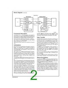
formation. When the Deserializer locks to the Bus LVDS
clock, the LOCK output will go low. When LOCK is low the
Deserializer outputs represent incoming Bus LVDS data.
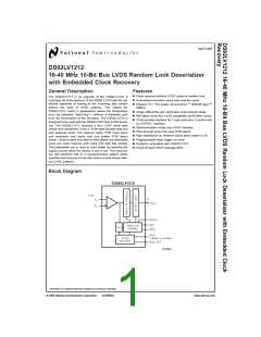
Functional Description
The DS92LV1212 is a 10-bit Deserializer chip designed to
receive data over a heavily loaded differential backplanes at
clock speeds from 16 MHz to 40 MHz. It may also be used to
receive data over Unshielded Twisted Pair (UTP) cable.
Data Transfer
Serialized data and clock bits (10+2 bits) are received at 12
times the TCLK frequency. For example, if TCLK is 40 MHz,
the serial rate is 40 x 12 = 480 Mega bits per second. Since
only 10 bits are from input data, the serial “payload” rate is
10 times the TCLK frequency. For instance, if TCLK = 40
MHz, the payload data rate is 40 x 10 = 400 Mbps. TCLK is
provided by the data source and must be in the range 16
MHz to 40 MHz nominal.
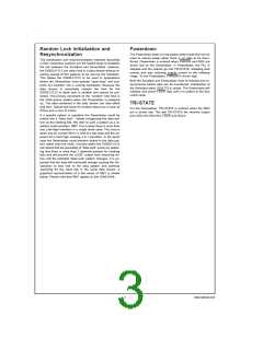
The chip has three active states of operation: Initialization,
Data Transfer, and Resynchronization; and two passive
states: Powerdown and TRI-STATE®.
The following sections describe each operation and passive
state.
Initialization
Before data can be transferred the Deserializer must be ini-
tialized. The Deserializer should be powered up with the
PWRDN pin held low. After VCC stabilizes the PWRDN pin
can be forced high. The Deserializer is ready to lock to the
incoming data stream.
The LOCK pin on the Deserializer is driven low when it is
synchronized with the Serializer. The Deserializer locks to
the embedded clock and uses it to recover the serialized
data. ROUT data is valid when LOCK is low. Otherwise
ROUT0–ROUT9 is invalid.
Step 1: When VCC is applied to the Deserializer, the respec-
tive outputs are held in TRI-STATE and internal circuitry is
disabled by on-chip power-on circuitry. When VCC reaches
VCC OK (2.5V) the PLL is ready to lock to incoming data or
synchronization patterns. The local clock is applied to the
REFCLK pin.
RCLK pin is the reference to data on the ROUT0-ROUT9
pins. The polarity of the RCLK edge is controlled by the
RCLK_R/F input.
ROUT(0-9), LOCK and RCLK outputs will drive a minimum
of three CMOS input gates (15 pF load) with 40 MHz clock.
The Deserializer LOCK output will remain high while its PLL
is locking to the incoming data or to SYNC patterns on the in-
put.
Resynchronization
The Deserializer LOCK pin driven low indicates that the De-
serializer PLL is locked to the embedded clock edge. If the
Deserializer loses lock, the LOCK output will go high and the
outputs (including RCLK) will be TRI-STATE.
Step 2: The Deserializer PLL must synchronize to the Serial-
izer to complete the initialization. The Deserializer will lock to
non-repetitive data patterns, however, the transmission of
SYNC patterns to the Deserializer enables the Deserializer
to lock to the Serializer signal within a specified time.
The LOCK pin must be monitored by the system to detect a
loss of synchronization. The system can arrange to pulse the
Serializer SYNC1 or SYNC2 pin to resynchronize. There are
multiple approaches possible. One recommendation is to
provide a feedback loop using the LOCK pin itself to control
the sync request of the Serializer (SYNC1 or SYNC2). A
minimum of 1024 sync patterns are needed to resynchro-
nize. Dual SYNC pins are provided for multiple control in a
multi-drop application.
Control of the Serializer SYNC1/2 pins is left to the user. A
feedback loop between the LOCK pin is one recommenda-
tion. Another option is that one or both of the Serializer
SYNC inputs are asserted for at least 1024 cycles of TCLK
to initiate transmission of SYNC patterns. The Serializer will
continue to send SYNC patterns after the minimum of 1024
if either of the SYNC inputs remain high.
When the Deserializer detects edge transitions at the Bus
LVDS input it will attempt to lock to the embedded clock in-
www.national.com
2

 NSC [ National Semiconductor ]