11.2 WATCHDOG/CLOCK MONITOR OPERATION
11.0 WATCHDOG/Clock Monitor
The WATCHDOG is enabled by bit 2 of the ECON register.
When this ECON bit is 0, the WATCHDOG is enabled and
pin G1 becomes the WATCHDOG output with a weak pullup.
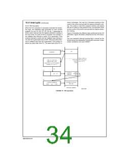
Each device contains a user selectable WATCHDOG and
clock monitor. The following section is applicable only if
WATCHDOG feature has been selected in the ECON regis-
ter. The WATCHDOG is designed to detect the user program
getting stuck in infinite loops resulting in loss of program con-
trol or “runaway” programs.
The WATCHDOG and Clock Monitor are disabled during re-
set. The device comes out of reset with the WATCHDOG
armed, the WATCHDOG Window Select bits (bits 6, 7 of the
WDSVR Register) set, and the Clock Monitor bit (bit 0 of the
WDSVR Register) enabled. Thus, a Clock Monitor error will
occur after coming out of reset, if the instruction cycle clock
frequency has not reached a minimum specified value, in-
cluding the case where the oscillator fails to start.
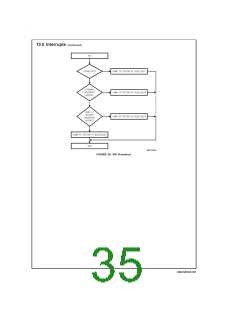
The WATCHDOG logic contains two separate service win-
dows. While the user programmable upper window selects
the WATCHDOG service time, the lower window provides
protection against an infinite program loop that contains the
WATCHDOG service instruction.
The WDSVR register can be written to only once after reset
and the key data (bits 5 through 1 of the WDSVR Register)
must match to be a valid write. This write to the WDSVR reg-
ister involves two irrevocable choices: (i) the selection of the
WATCHDOG service window (ii) enabling or disabling of the
Clock Monitor. Hence, the first write to WDSVR Register in-
volves selecting or deselecting the Clock Monitor, select the
WATCHDOG service window and match the WATCHDOG
key data. Subsequent writes to the WDSVR register will
compare the value being written by the user to the WATCH-
DOG service window value and the key data (bits 7 through
1) in the WDSVR Register. Table 9 shows the sequence of
events that can occur.
The Clock Monitor is used to detect the absence of a clock or
a very slow clock below a specified rate on the CKI pin.
The WATCHDOG consists of two independent logic blocks:
WD UPPER and WD LOWER. WD UPPER establishes the
upper limit on the service window and WD LOWER defines
the lower limit of the service window.
Servicing the WATCHDOG consists of writing a specific
value to a WATCHDOG Service Register named WDSVR
which is memory mapped in the RAM. This value is com-
posed of three fields, consisting of a 2-bit Window Select, a
5-bit Key Data field, and the 1-bit Clock Monitor Select field.
Table 7 shows the WDSVR register.
The user must service the WATCHDOG at least once before
the upper limit of the service window expires. The WATCH-
DOG may not be serviced more than once in every lower
limit of the service window.
TABLE 7. WATCHDOG Service Register (WDSVR)
Window
Select
Clock
Key Data
Monitor
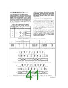
The WATCHDOG has an output pin associated with it. This
is the WDOUT pin, on pin 1 of the port G. WDOUT is active
low and must be externally connected to the RESET pin or to
some other external logic which handles WATCHDOG event.
The WDOUT pin has a weak pullup in the inactive state. This
pull-up is sufficient to serve as the connection to VCC for sys-
tems which use the internal Power On Reset. Upon trigger-
ing the WATCHDOG, the logic will pull the WDOUT (G1) pin
low for an additional 16 tC–32 tC cycles after the signal level
on WDOUT pin goes below the lower Schmitt trigger thresh-
old. After this delay, the device will stop forcing the WDOUT
output low. The WATCHDOG service window will restart
when the WDOUT pin goes high.
X
7
X
6
0
5
1
4
1
3
0
2
0
1
Y
0
The lower limit of the service window is fixed at 256 instruc-
tion cycles. Bits 7 and 6 of the WDSVR register allow the
user to pick an upper limit of the service window.
Table 8 shows the four possible combinations of lower and
upper limits for the WATCHDOG service window. This flex-
ibility in choosing the WATCHDOG service window prevents
any undue burden on the user software.
Bits 5, 4, 3, 2 and 1 of the WDSVR register represent the
5-bit Key Data field. The key data is fixed at 01100. Bit 0 of
the WDSVR Register is the Clock Monitor Select bit.
A WATCHDOG service while the WDOUT signal is active will
be ignored. The state of the WDOUT pin is not guaranteed
on reset, but if it powers up low then the WATCHDOG will
time out and WDOUT will go high.
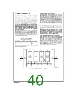
TABLE 8. WATCHDOG Service Window Select
WDSVR WDSVR
Clock
Service Window
(Lower-Upper Limits)
2048–8k tC Cycles
The Clock Monitor forces the G1 pin low upon detecting a
clock frequency error. The Clock Monitor error will continue
until the clock frequency has reached the minimum specified
value, after which the G1 output will go high following 16
tC–32 tC clock cycles. The Clock Monitor generates a con-
tinual Clock Monitor error if the oscillator fails to start, or fails
to reach the minimum specified frequency. The specification
for the Clock Monitor is as follows:
Bit 7
Bit 6
Monitor
0
0
1
1
x
x
0
1
0
1
x
x
x
x
x
x
0
1
2048–16k tC Cycles
2048–32k tC Cycles
2048–64k tC Cycles
Clock Monitor Disabled
Clock Monitor Enabled
>
1/tC 10 kHz — No clock rejection.
<
1/tC 10 Hz — Guaranteed clock rejection.
11.1 CLOCK MONITOR
The Clock Monitor aboard the device can be selected or de-
selected under program control. The Clock Monitor is guar-
anteed not to reject the clock if the instruction cycle clock (1/
tC) is greater or equal to 10 kHz. This equates to a clock
input rate on CKI of greater or equal to 100 kHz.
www.national.com
38

 NSC [ National Semiconductor ]