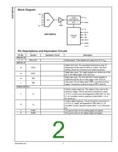
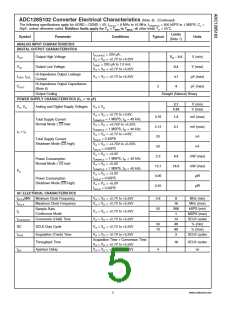
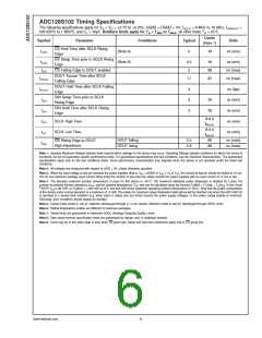
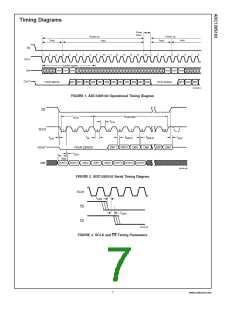
ADC128S102 Timing Specifications
The following specifications apply for VA = VD = +2.7V to +5.25V, AGND = DGND = 0V, fSCLK = 8 MHz to 16 MHz, fSAMPLE
=
500 kSPS to 1 MSPS, and CL = 50pF. Boldface limits apply for TA = TMIN to TMAX: all other limits TA = 25˚C.
Limits
(Note 7)
Symbol
Parameter
Conditions
Typical
Units
CS Hold Time after SCLK Rising
Edge
tCSH
(Note 9)
(Note 9)
0
10
ns (min)
CS Setup Time prior to SCLK Rising
Edge
tCSS
tEN
4.5
5
10
30
27
ns (min)
ns (max)
ns (max)
CS Falling Edge to DOUT enabled
DOUT Access Time after SCLK
Falling Edge
tDACC
17
DOUT Hold Time after SCLK Falling
Edge
tDHLD
tDS
4
3
3
ns (typ)
ns (min)
ns (min)
ns (min)
ns (min)
DIN Setup Time prior to SCLK
Rising Edge
10
10
DIN Hold Time after SCLK Rising
Edge
tDH
0.4 x
tSCLK
0.4 x
tSCLK
20
tCH
SCLK High Time
SCLK Low Time
tCL
DOUT falling
DOUT rising
2.4
0.9
ns (max)
ns (max)
CS Rising Edge to DOUT
High-Impedance
tDIS
20
Note 1: Absolute Maximum Ratings indicate limits beyond which damage to the device may occur. Operating Ratings indicate conditions for which the device is
functional, but do not guarantee specific performance limits. For guaranteed specifications and test conditions, see the Electrical Characteristics. The guaranteed
specifications apply only for the test conditions listed. Some performance characteristics may degrade when the device is not operated under the listed test
conditions.
Note 2: All voltages are measured with respect to GND = 0V, unless otherwise specified.
<
>
V
A
Note 3: When the input voltage at any pin exceeds the power supplies (that is, V
AGND or V
or V ), the current at that pin should be limited to 10 mA.
D
IN
IN
The 20 mA maximum package input current rating limits the number of pins that can safely exceed the power supplies with an input current of 10 mA to two.
Note 4: The absolute maximum junction temperature (T max) for this device is 150˚C. The maximum allowable power dissipation is dictated by T max, the
J
J
junction-to-ambient thermal resistance (θ ), and the ambient temperature (T ), and can be calculated using the formula P MAX = (T max − T )/θ . In the 16-pin
JA
A
D
J
A
JA
TSSOP, θ is 96˚C/W, so P MAX = 1,200 mW at 25˚C and 625 mW at the maximum operating ambient temperature of 105˚C. Note that the power consumption
JA
D
of this device under normal operation is a maximum of 12 mW. The values for maximum power dissipation listed above will be reached only when the ADC128S102
is operated in a severe fault condition (e.g. when input or output pins are driven beyond the power supply voltages, or the power supply polarity is reversed).
Obviously, such conditions should always be avoided.
Note 5: Human body model is 100 pF capacitor discharged through a 1.5 kΩ resistor. Machine model is 220 pF discharged through ZERO ohms
Note 6: Reflow temperature profiles are different for lead-free packages.
Note 7: Tested limits are guaranteed to National’s AOQL (Average Outgoing Quality Level).
Note 8: Data sheet min/max specification limits are guaranteed by design, test, or statistical analysis.
Note 9: Clock may be in any state (high or low) when CS goes high. Setup and hold time restrictions apply only to CS going low.
www.national.com
6

 NSC [ National Semiconductor ]