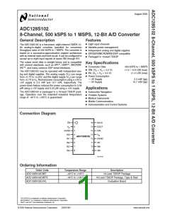
Block Diagram
20136107
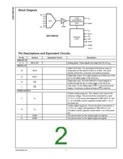
Pin Descriptions and Equivalent Circuits
Pin No.
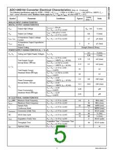
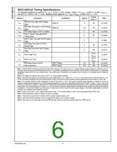
ANALOG I/O
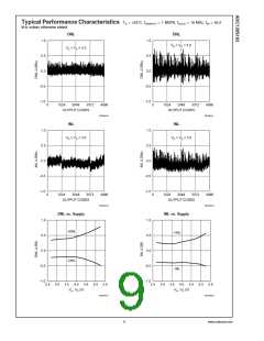
4 - 11
Symbol
Equivalent Circuit
Description
IN0 to IN7
Analog inputs. These signals can range from 0V to VREF.
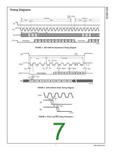
DIGITAL I/O
Digital clock input. The guaranteed performance range of
frequencies for this input is 8 MHz to 16 MHz. This clock
directly controls the conversion and readout processes.
Digital data output. The output samples are clocked out of this
pin on the falling edges of the SCLK pin.
16
SCLK
15
14
DOUT
DIN
Digital data input. The ADC128S102’s Control Register is
loaded through this pin on rising edges of the SCLK pin.
Chip select. On the falling edge of CS, a conversion process
begins. Conversions continue as long as CS is held low.
1
CS
POWER SUPPLY
Positive analog supply pin. This voltage is also used as the
reference voltage. This pin should be connected to a quiet
+2.7V to +5.25V source and bypassed to GND with 1 µF and
0.1 µF monolithic ceramic capacitors located within 1 cm of
the power pin.
2
VA
Positive digital supply pin. This pin should be connected to a
+2.7V to VA supply, and bypassed to GND with a 0.1 µF
monolithic ceramic capacitor located within 1 cm of the power
pin.
13
VD
3
AGND
DGND
The ground return for the analog supply and signals.
The ground return for the digital supply and signals.
12
www.national.com
2

 NSC [ National Semiconductor ]