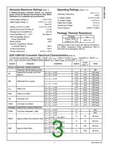
Absolute Maximum Ratings (Note 1)
Operating Ratings (Notes 1, 2)
If Military/Aerospace specified devices are required,
please contact the National Semiconductor Sales Office/
Distributors for availability and specifications.
−40˚C ≤ TA
≤
Operating Temperature
+105˚C
+2.7V to +5.25V
+2.7V to VA
0V to VA
VA Supply Voltage
VD Supply Voltage
Digital Input Voltage
Analog Input Voltage
Analog Supply Voltage VA
Digital Supply Voltage VD
−0.3V to 6.5V
−0.3V to VA + 0.3V,
max 6.5V
0V to VA
Voltage on Any Pin to GND
Input Current at Any Pin (Note 3)
Package Input Current(Note 3)
Power Dissipation at TA = 25˚C
ESD Susceptibility (Note 5)
Human Body Model
−0.3V to VA +0.3V
10 mA
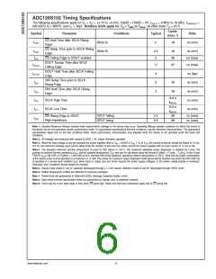
Clock Frequency
8 MHz to 16 MHz
20 mA
Package Thermal Resistance
See (Note 4)
Package
θJA
16-lead TSSOP on
4-layer, 2 oz. PCB
2500V
250V
96˚C / W
Machine Model
Soldering Temperature, Infrared,
10 seconds (Note 6)
Soldering process must comply with National Semiconduc-
tor’s Reflow Temperature Profile specifications. Refer to
www.national.com/packaging. (Note 6)
260˚C
+150˚C
Junction Temperature
Storage Temperature
−65˚C to +150˚C
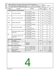
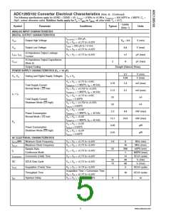
ADC128S102 Converter Electrical Characteristics (Note 8)
The following specifications apply for AGND = DGND = 0V, fSCLK = 8 MHz to 16 MHz, fSAMPLE = 500 kSPS to 1 MSPS, CL
=
50pF, unless otherwise noted. Boldface limits apply for TA = TMIN to TMAX: all other limits TA = 25˚C.
Limits
(Note 7)
Symbol
Parameter
Conditions
Typical
Units
STATIC CONVERTER CHARACTERISTICS
Resolution with No Missing Codes
12
1
Bits
VA = VD = +3.0V
0.4
0.5
LSB (max)
LSB (max)
LSB (max)
LSB (min)
LSB (max)
LSB (min)
LSB (max)
LSB (max)
LSB (max)
LSB (max)
LSB (max)
LSB (max)
LSB (max)
LSB (max)
Integral Non-Linearity (End Point
INL
Method)
VA = VD = +5.0V
1.2
+0.9
−0.7
+1.5
−0.9
2.3
2.3
1.5
1.5
2.0
2.0
1.5
1.5
+0.4
−0.2
+0.7
−0.4
+0.8
+1.1
0.1
VA = VD = +3.0V
DNL
Differential Non-Linearity
VA = VD = +5.0V
VA = VD = +3.0V
VA = VD = +5.0V
VA = VD = +3.0V
VA = VD = +5.0V
VA = VD = +3.0V
VA = VD = +5.0V
VA = VD = +3.0V
VA = VD = +5.0V
VOFF
OEM
FSE
Offset Error
Offset Error Match
Full Scale Error
Full Scale Error Match
0.3
+0.8
+0.3
0.1
FSEM
0.3
DYNAMIC CONVERTER CHARACTERISTICS
VA = VD = +3.0V
8
MHz
MHz
FPBW
Full Power Bandwidth (−3dB)
VA = VD = +5.0V
11
VA = VD = +3.0V,
73
73
73
73
70
70
dB (min)
dB (min)
dB (min)
dB (min)
fIN = 40.2 kHz, −0.02 dBFS
VA = VD = +5.0V,
SINAD
Signal-to-Noise Plus Distortion Ratio
fIN = 40.2 kHz, −0.02 dBFS
VA = VD = +3.0V,
70.8
70.8
fIN = 40.2 kHz, −0.02 dBFS
VA = VD = +5.0V,
SNR
Signal-to-Noise Ratio
fIN = 40.2 kHz, −0.02 dBFS
3
www.national.com

 NSC [ National Semiconductor ]