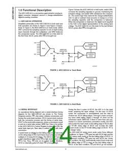
close to the ADC128S102. The digital supply is separated
from the analog supply by an isolation resistor and bypassed
with additional capacitors. The ADC128S102 uses the ana-
log supply (VA) as its reference voltage, so it is very impor-
tant that VA be kept as clean as possible. Due to the low
power requirements of the ADC128S102, it is also possible
to use a precision reference as a power supply.
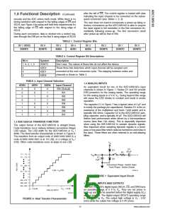
2.0 Applications Information
2.1 TYPICAL APPLICATION CIRCUIT
A typical application is shown in Figure 8. The split analog
and digital supply pins are both powered in this example by
the National LP2950 low-dropout voltage regulator. The ana-
log supply is bypassed with a capacitor network located
20136113
FIGURE 8. Typical Application Circuit
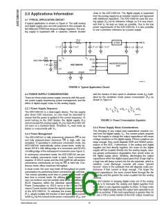
2.2 POWER SUPPLY CONSIDERATIONS
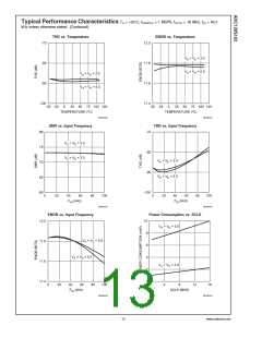
add the fraction of time spent in shutdown mode (tS) multi-
plied by the shutdown mode power consumption (PS) as
shown in Figure 9.
There are three major power supply concerns with this prod-
uct: power supply sequencing, power management, and the
effect of digital supply noise on the analog supply.
2.2.1 Power Supply Sequence
The ADC128S102 is a dual-supply device. The two supply
pins share ESD resources, so care must be exercised to
ensure that the power is applied in the correct sequence. To
avoid turning on the ESD diodes, the digital supply (VD)
cannot exceed the analog supply (VA) by more than 300 mV,
not even on a transient basis. Therefore, VA must ramp up
before or concurrently with VD.
20136115
FIGURE 9. Power Consumption Equation
2.2.3 Power Supply Noise Considerations
The charging of any output load capacitance requires cur-
rent from the digital supply, VD. The current pulses required
from the supply to charge the output capacitance will cause
voltage variations on the digital supply. If these variations are
large enough, they could degrade SNR and SINAD perfor-
mance of the ADC. Furthermore, if the analog and digital
supplies are tied directly together, the noise on the digital
supply will be coupled directly into the analog supply, caus-
ing greater performance degradation than would noise on
the digital supply alone. Similarly, discharging the output
capacitance when the digital output goes from a logic high to
a logic low will dump current into the die substrate, which is
resistive. Load discharge currents will cause "ground
bounce" noise in the substrate that will degrade noise per-
formance if that current is large enough. The larger the
output capacitance, the more current flows through the die
substrate and the greater the noise coupled into the analog
channel.
2.2.2 Power Management
The ADC128S102 is fully powered-up whenever CS is low
and fully powered-down whenever CS is high, with one
exception. If operating in continuous conversion mode, the
ADC128S102 automatically enters power-down mode be-
tween SCLK’s 16th falling edge of a conversion and SCLK’s
1st falling edge of the subsequent conversion (see Figure 1).
In continuous conversion mode, the ADC128S102 can per-
form multiple conversions back to back. Each conversion
requires 16 SCLK cycles and the ADC128S102 will perform
conversions continuously as long as CS is held low. Con-
tinuous mode offers maximum throughput.
In burst mode, the user may trade off throughput for power
consumption by performing fewer conversions per unit time.
This means spending more time in power-down mode and
less time in normal mode. By utilizing this technique, the
user can achieve very low sample rates while still utilizing an
SCLK frequency within the electrical specifications. The
Power Consumption vs. SCLK curve in the Typical Perfor-
mance Curves section shows the typical power consumption
of the ADC128S102. To calculate the power consumption
(PC), simply multiply the fraction of time spent in the normal
mode (tN) by the normal mode power consumption (PN), and
The first solution to keeping digital noise out of the analog
supply is to decouple the analog and digital supplies from
each other or use separate supplies for them. To keep noise
out of the digital supply, keep the output load capacitance as
small as practical. If the load capacitance is greater than 50
pF, use a 100 Ω series resistor at the ADC output, located as
www.national.com
16

 NSC [ National Semiconductor ]