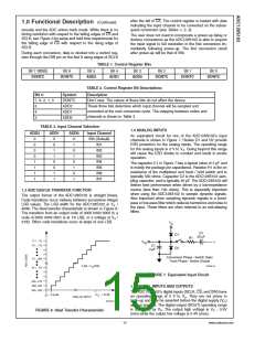
Figure 5 shows the ADC128S102 in hold mode: switch SW1
connects the sampling capacitor to ground, maintaining the
sampled voltage, and switch SW2 unbalances the compara-
tor. The control logic then instructs the charge-redistribution
DAC to add or subtract fixed amounts of charge to or from
the sampling capacitor until the comparator is balanced.
When the comparator is balanced, the digital word supplied
to the DAC is the digital representation of the analog input
voltage. The ADC128S102 is in this state for the last thirteen
SCLK cycles after CS is brought low.
1.0 Functional Description
The ADC128S102 is a successive-approximation analog-to-
digital converter designed around a charge-redistribution
digital-to-analog converter.
1.1 ADC128S102 OPERATION
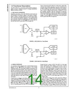
Simplified schematics of the ADC128S102 in both track and
hold operation are shown in Figure 4 and Figure 5 respec-
tively. In Figure 4, the ADC128S102 is in track mode: switch
SW1 connects the sampling capacitor to one of eight analog
input channels through the multiplexer, and SW2 balances
the comparator inputs. The ADC128S102 is in this state for
the first three SCLK cycles after CS is brought low.
20136109
FIGURE 4. ADC128S102 in Track Mode
20136110
FIGURE 5. ADC128S102 in Hold Mode
1.2 SERIAL INTERFACE
During the first 3 cycles of SCLK, the ADC is in the track
mode, acquiring the input voltage. For the next 13 SCLK
cycles the conversion is accomplished and the data is
clocked out. SCLK falling edges 1 through 4 clock out lead-
ing zeros while falling edges 5 through 16 clock out the
conversion result, MSB first. If there is more than one con-
version in a frame (continuous conversion mode), the ADC
will re-enter the track mode on the falling edge of SCLK after
the N*16th rising edge of SCLK and re-enter the hold/
convert mode on the N*16+4th falling edge of SCLK. "N" is
an integer value.
An operational timing diagram and a serial interface timing
diagram for the ADC128S102 are shown in The Timing
Diagrams section. CS, chip select, initiates conversions and
frames the serial data transfers. SCLK (serial clock) controls
both the conversion process and the timing of serial data.
DOUT is the serial data output pin, where a conversion result
is sent as a serial data stream, MSB first. Data to be written
to the ADC128S102’s Control Register is placed on DIN, the
serial data input pin. New data is written to DIN with each
conversion.
The ADC128S102 enters track mode under three different
conditions. In Figure 1, CS goes low with SCLK high and the
ADC enters track mode on the first falling edge of SCLK. In
the second condition, CS goes low with SCLK low. Under
this condition, the ADC automatically enters track mode and
the falling edge of CS is seen as the first falling edge of
SCLK. In the third condition, CS and SCLK go low simulta-
A serial frame is initiated on the falling edge of CS and ends
on the rising edge of CS. Each frame must contain an integer
multiple of 16 rising SCLK edges. The ADC’s DOUT pin is in
a high impedance state when CS is high and is active when
CS is low. Thus, CS acts as an output enable. Similarly,
SCLK is internally gated off when CS is brought high.
www.national.com
14

 NSC [ National Semiconductor ]