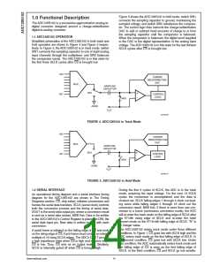
after the fall of CS. The control register is loaded with data
indicating the input channel to be converted on the subse-
quent conversion (see Tables 1, 2, 3).
1.0 Functional Description (Continued)
neously and the ADC enters track mode. While there is no
timing restriction with respect to the falling edges of CS and
SCLK, see Figure 3 for setup and hold time requirements for
the falling edge of CS with respect to the rising edge of
SCLK.
The user does not need to incorporate a power-up delay or
dummy conversions as the ADC128S102 is able to acquire
the input signal to full resolution in the first conversion im-
mediately following power-up. The first conversion result
after power-up will be that of IN0.
During each conversion, data is clocked into a control reg-
ister through the DIN pin on the first 8 rising edges of SCLK
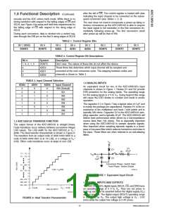
TABLE 1. Control Register Bits
Bit 4 Bit 3
ADD1 ADD0
Bit 7 (MSB)
Bit 6
Bit 5
Bit 2
Bit 1
Bit 0
DONTC
DONTC
ADD2
DONTC
DONTC
DONTC
TABLE 2. Control Register Bit Descriptions
Description
Bit #:
Symbol:
DONTC
ADD2
7, 6, 2, 1, 0
Don’t care. The values of these bits do not affect the device.
These three bits determine which input channel will be sampled and
converted at the next conversion cycle. The mapping between codes and
channels is shown in Table 3.
5
4
3
ADD1
ADD0
TABLE 3. Input Channel Selection
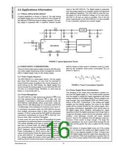
1.4 ANALOG INPUTS
ADD2
ADD1
ADD0
Input Channel
An equivalent circuit for one of the ADC128S102’s input
channels is shown in Figure 7. Diodes D1 and D2 provide
ESD protection for the analog inputs. The operating range
for the analog inputs is 0 V to VA. Going beyond this range
will cause the ESD diodes to conduct and result in erratic
operation.
0
0
0
0
1
1
1
1
0
0
1
1
0
0
1
1
0
1
0
1
0
1
0
1
IN0 (Default)
IN1
IN2
IN3
IN4
IN5
IN6
IN7
The capacitor C1 in Figure 7 has a typical value of 3 pF and
is mainly the package pin capacitance. Resistor R1 is the on
resistance of the multiplexer and track / hold switch and is
typically 500 ohms. Capacitor C2 is the ADC128S102 sam-
pling capacitor, and is typically 30 pF. The ADC128S102 will
deliver best performance when driven by a low-impedance
source (less than 100 ohms). This is especially important
when using the ADC128S102 to sample dynamic signals.
Also important when sampling dynamic signals is a band-
pass or low-pass filter which reduces harmonics and noise in
the input. These filters are often referred to as anti-aliasing
filters.
1.3 ADC128S102 TRANSFER FUNCTION
The output format of the ADC128S102 is straight binary.
Code transitions occur midway between successive integer
LSB values. The LSB width for the ADC128S102 is VA
4096. The ideal transfer characteristic is shown in Figure 6.
The transition from an output code of 0000 0000 0000 to a
/
code of 0000 0000 0001 is at 1/2 LSB, or a voltage of VA
8192. Other code transitions occur at steps of one LSB.
/
20136114
FIGURE 7. Equivalent Input Circuit
1.5 DIGITAL INPUTS AND OUTPUTS
The ADC128S102’s digital inputs (SCLK, CS, and DIN) have
an operating range of 0 V to VA. They are not prone to
latch-up and may be asserted before the digital supply (VD)
without any risk. The digital output (DOUT) operating range
is controlled by VD. The output high voltage is VD - 0.5V
(min) while the output low voltage is 0.4V (max).
20136111
FIGURE 6. Ideal Transfer Characteristic
15
www.national.com

 NSC [ National Semiconductor ]