74VHC541; 74VHCT541
Nexperia
Octal buffer/line driver; 3-state
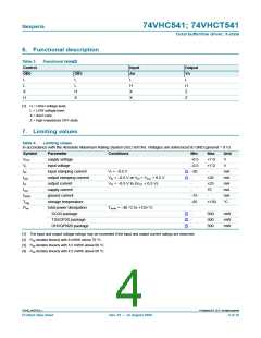
6. Functional description
Table 3.
Functional table[1]
Control
Input
An
L
Output
OE0
L
OE1
Yn
L
L
L
L
H
H
Z
X
H
X
X
H
X
Z
[1] H = HIGH voltage level;
L = LOW voltage level;
X = don’t care;
Z = high-impedance OFF-state.
7. Limiting values
Table 4.
Limiting values
In accordance with the Absolute Maximum Rating System (IEC 60134). Voltages are referenced to GND (ground = 0 V).
Symbol
VCC
VI
Parameter
Conditions
Min
−0.5
−0.5
−20
-
Max
+7.0
+7.0
-
Unit
V
supply voltage
input voltage
V
[1]
[1]
IIK
input clamping current
output clamping current
output current
VI < −0.5 V
mA
mA
mA
mA
mA
°C
IOK
VO < −0.5 V or VO > VCC + 0.5 V
VO = −0.5 V to (VCC + 0.5 V)
±20
±25
75
IO
-
ICC
supply current
-
IGND
Tstg
Ptot
ground current
−75
−65
-
storage temperature
total power dissipation
SO20 package
+150
Tamb = −40 °C to +125 °C
[2]
[3]
[4]
-
-
-
500
500
500
mW
mW
mW
TSSOP20 package
DHVQFN20 package
[1] The input and output voltage ratings may be exceeded if the input and output current ratings are observed.
[2] Ptot derates linearly with 8 mW/K above 70 °C.
[3] Ptot derates linearly with 5.5 mW/K above 60 °C.
[4] Ptot derates linearly with 4.5 mW/K above 60 °C.
©
74VHC_VHCT541_1
Nexperia B.V. 2017. All rights reserved
Product data sheet
Rev. 01 — 12 August 2009
4 of 16

 NEXPERIA [ Nexperia ]