74VHC541; 74VHCT541
Nexperia
Octal buffer/line driver; 3-state
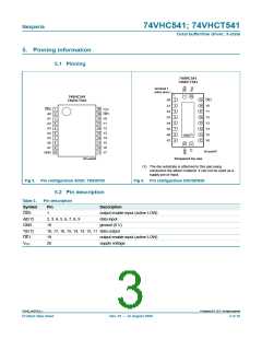
5. Pinning information
5.1 Pinning
74VHC541
74VHCT541
terminal 1
index area
74VHC541
74VHCT541
2
3
4
5
6
7
8
9
19
18
17
16
15
14
13
12
A0
A1
A2
A3
A4
A5
A6
A7
OE1
Y0
Y1
Y2
Y3
Y4
Y5
Y6
1
2
20
19
18
17
16
15
14
13
12
11
OE0
A0
V
CC
OE1
Y0
Y1
Y2
Y3
Y4
Y5
Y6
Y7
3
A1
4
A2
5
A3
6
A4
(1)
GND
7
A5
8
A6
9
A7
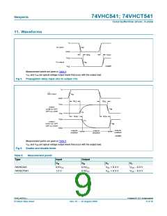
001aak047
10
GND
Transparent top view
001aak046
(1) The die substrate is attached to this pad using
conductive die attach material. It can not be used as a
supply pin or input.
Fig 3. Pin configuration SO20, TSSOP20
Fig 4. Pin configuration DHVQFN20
5.2 Pin description
Table 2.
Symbol
OE0
Pin description
Pin
Description
1
output enable input (active LOW)
data input
A[0:7]
GND
2, 3, 4, 5, 6, 7, 8, 9
10
ground (0 V)
Y[0:7]
OE1
18, 17, 16, 15, 14, 13, 12, 11 data output
19
20
output enable input (active LOW)
supply voltage
VCC
©
74VHC_VHCT541_1
Nexperia B.V. 2017. All rights reserved
Product data sheet
Rev. 01 — 12 August 2009
3 of 16

 NEXPERIA [ Nexperia ]