74HC4511; 74HCT4511
Nexperia
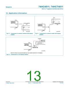
BCD to 7-segment latch/decoder/driver
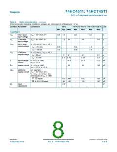
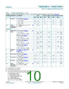
10. Dynamic characteristics
Table 7.
Dynamic characteristics
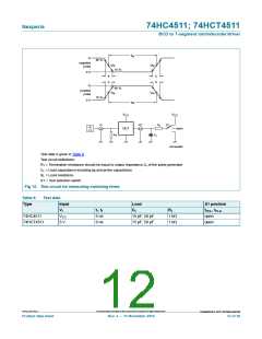
Voltages are referenced to GND (ground = 0 V); CL = 50 pF unless otherwise specified; for test circuit see Figure 12.
Symbol Parameter Conditions
74HC4511
25 C
40 C to +85 C 40 C to +125 C Unit
Min Typ Max
Min
Max
Min
Max
[1]
tpd
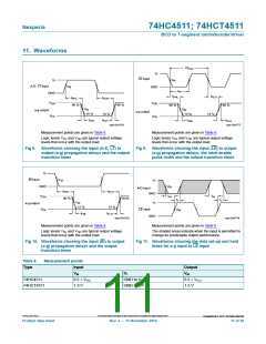
propagation A-D to a-g; see Figure 8
delay
VCC = 2.0 V
-
-
-
-
77
28
24
22
300
60
-
-
-
-
-
375
75
-
-
-
-
-
450
90
-
ns
ns
ns
ns
VCC = 4.5 V
VCC = 5.0 V; CL = 15 pF
VCC = 6.0 V
51
64
77
LE to a-g; see Figure 9
VCC = 2.0 V
-
-
-
-
74
27
23
22
270
54
-
-
-
-
-
330
68
-
-
-
-
-
405
81
-
ns
ns
ns
ns
VCC = 4.5 V
VCC = 5.0 V; CL = 15 pF
VCC = 6.0 V
46
58
69
BI to a-g; see Figure 10
VCC = 2.0 V
-
-
-
-
61
22
19
18
220
44
-
-
-
-
-
275
55
-
-
-
-
-
330
66
-
ns
ns
ns
ns
VCC = 4.5 V
VCC = 5.0 V; CL = 15 pF
VCC = 6.0 V
37
47
56
LT to a-g; see Figure 8
VCC = 2.0 V
-
-
-
-
41
15
12
12
150
30
-
-
-
-
-
190
38
-
-
-
-
-
225
45
-
ns
ns
ns
ns
VCC = 4.5 V
VCC = 5.0 V; CL = 15 pF
VCC = 6.0 V
26
33
38
[2]
tt
transition
time
see Figure 8, Figure 9 and
Figure 10
VCC = 2.0 V
VCC = 4.5 V
VCC = 6.0 V
-
-
-
19
7
75
15
13
-
-
-
95
19
16
-
-
-
110
22
ns
ns
ns
6
19
tW
pulse width LE LOW; see Figure 9
VCC = 2.0 V
80
16
14
11
4
-
-
-
100
20
-
-
-
120
24
-
-
-
ns
ns
ns
VCC = 4.5 V
VCC = 6.0 V
3
17
20
tsu
set-up time A-D to LE; see Figure 11
VCC = 2.0 V
60
12
10
14
5
-
-
-
75
15
13
-
-
-
90
18
15
-
-
-
ns
ns
ns
VCC = 4.5 V
VCC = 6.0 V
4
74HC_HCT4511
All information provided in this document is subject to legal disclaimers.
©
Nexperia B.V. 2017. All rights reserved
Product data sheet
Rev. 3 — 15 November 2016
9 of 18

 NEXPERIA [ Nexperia ]