Nexperia
74HC253; 74HCT253
Dual 4-input multiplexer; 3-state
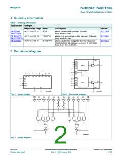
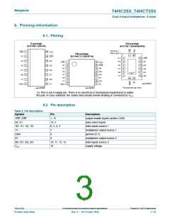
6. Pinning information
6.1. Pinning
D package
BQ package
SOT109-1 (SO16)
SOT763-1 (DHVQFN16)
terminal 1
index area
1
2
3
4
5
6
7
8
16
V
1OE
S1
CC
PW package
SOT403-1 (TSSOP16)
15
14
13
12
11
10
9
2OE
S0
2
3
4
5
6
7
15
14
13
12
11
10
S1
1I3
1I2
1I1
1I0
1Y
2OE
S0
1I3
1
2
3
4
5
6
7
8
16
15
14
13
12
11
10
9
1OE
S1
V
CC
2I3
2I2
2I1
2I0
2OE
S0
1I2
2I3
2I2
2I1
2I0
2Y
1I3
1I1
1I2
2I3
2I2
2I1
2I0
2Y
(1)
CC
V
1I1
1I0
1I0
1Y
1Y
aaa-034032
GND
GND
Transparent top view
aaa-035486
aaa-035487
(1) This is not a supply pin. There is no electrical or mechanical requirement to solder
the pad. In case soldered, the solder land should remain floating or connected to VCC
.
6.2. Pin description
Table 2. Pin description
Symbol
Pin
Description
1OE, 2OE
1, 15
output enable inputs (active LOW)
data select inputs
S0, S1
14, 2
1I0, 1I1, 1I2, 1I3
6, 5, 4, 3
data inputs source 1
multiplexer output source 1
ground (0 V)
1Y
7
GND
8
2Y
9
multiplexer output source 2
data inputs source 2
supply voltage
2I0, 2I1, 2I2, 2I3
VCC
10, 11, 12, 13
16
©
74HC_HCT253
All information provided in this document is subject to legal disclaimers.
Nexperia B.V. 2022. All rights reserved
Product data sheet
Rev. 9 — 20 October 2022
3 / 16

 NEXPERIA [ Nexperia ]