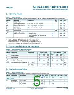
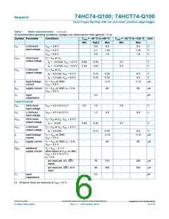
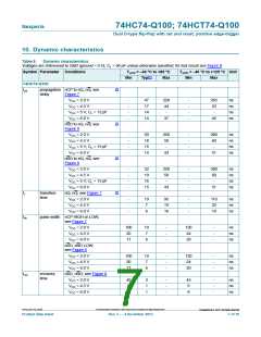
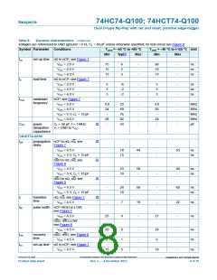
74HC74-Q100; 74HCT74-Q100
Nexperia
Dual D-type flip-flop with set and reset; positive edge-trigger
4
&
&
&
&
&
&
&
4
&
'
5'
6'
&3
PQDꢀꢄꢁ
&
&
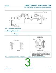
Fig 4. Logic diagram for one flip-flop
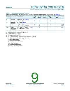
5. Pinning information
5.1 Pinning
ꢀꢁ+&ꢀꢁꢂ4ꢃꢄꢄ
ꢀꢁ+&7ꢀꢁꢂ4ꢃꢄꢄ
WHUPLQDOꢊꢁ
LQGH[ꢊDUHD
ꢀꢁ+&ꢀꢁꢂ4ꢃꢄꢄ
ꢀꢁ+&7ꢀꢁꢂ4ꢃꢄꢄ
ꢃ
ꢆ
ꢀ
ꢄ
ꢇ
ꢁꢆ
ꢁꢃ
ꢁꢁ
ꢁꢂ
ꢅ
ꢁ'
ꢁ&3
ꢁ6'
ꢁ4
ꢃ5'
ꢃ'
ꢁ
ꢃ
ꢆ
ꢀ
ꢄ
ꢇ
ꢉ
ꢁꢀ
ꢁꢆ
ꢁꢃ
ꢁꢁ
ꢁꢂ
ꢅ
ꢁ5'
ꢁ'
9
&&
ꢃ5'
ꢃ'
ꢃ&3
ꢃ6'
ꢃ4
ꢁ&3
ꢁ6'
ꢁ4
ꢋꢁꢌ
*1'
ꢃ&3
ꢃ6'
ꢃ4
ꢁ4
ꢁ4
DDDꢆꢅꢅꢀꢇꢃꢉ
*1'
ꢈ
ꢃ4
7UDQVSDUHQWꢊWRSꢊYLHZ
DDDꢆꢅꢅꢀꢇꢃꢈ
(1) This is not a supply pin. The substrate is attached to this
pad using conductive die attach material. There is no
electrical or mechanical requirement to solder this pad.
However, if it is soldered, the solder land should remain
floating or be connected to GND.
Fig 5. Pin configuration for SO14 and TSSOP14
Fig 6. Pin configuration for DHVQFN14
74HC_HCT74_Q100
All information provided in this document is subject to legal disclaimers.
©
Nexperia B.V. 2017. All rights reserved
Product data sheet
Rev. 3 — 4 December 2015
3 of 19

 NEXPERIA [ Nexperia ]