µPD75304B,75306B,75308B
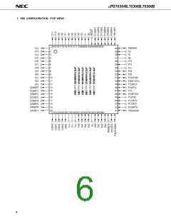
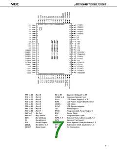
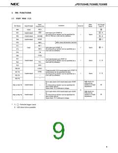
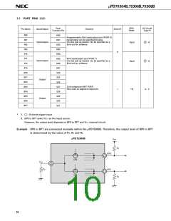
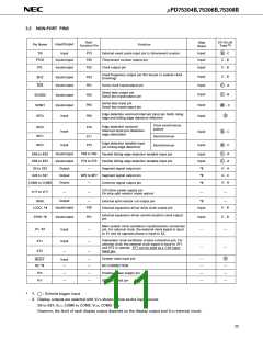
3. PIN FUNCTIONS
3.1 PORT PINS (1/2)
Dual-
Function Pin
After
Reset
I/O Circuit
Type *1
Function
Pin Name
Input/Output
8-bit I/O
INT4
SCK
SO/SB0
SI/SB1
INT0
INT1
INT2
TI0
B
P00
P01
Input
4-bit input port (PORT 0)
On-chip pull-up resistor can be specified for
P01 to P03 as a 3-bit unit by software.
F - A
F - B
M - C
Input/output
Input/output
Input/output
×
Input
Input
Input
Input
P02
P03
With noise elimination function
P10
P11
4-bit input port (PORT 1)
On-chip pull-up resistor can be specified as a
4-bit unit by software.
B - C
E - B
E - B
Input
×
×
×
P12
P13
PTO0
—
P20
P21
4-bit input/output port (PORT 2)
On-chip pull-up resistor can be specified as a
4-bit unit by software.
Input/output
Input/output
PCL
P22
BUZ
LCDCL
SYNC
—
P23
P30 *2
P31 *2
P32 *2
P33 *2
Programmable 4-bit input/output port (PORT 3)
Input/output can be specified bit-wise.
On-chip pull-up resistor can be specified as a
4-bit unit by software.
—
High level (on-
chip pull-up
resistor) or high-
impedance
N-ch open-drain 4-bit input/output port (PORT
4)
On-chip pull-up resistor can be specified bit-
wise (mask option).
—
—
M
M
Input/output
Input/output
P40 to P43 *2
P50 to P53 *2
Open-drain: 10 V withstand voltage
High level (on-
chip pull-up
resistor) or high-
impedance
N-ch open-drain 4-bit input/output port (PORT
5)
On-chip pull-up resistor can be specified bit-
wise (mask option).
Open-drain: 10 V withstand voltage
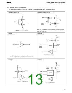
*
1.
: Schmitt trigger input
2. LED direct drive possible
9

 NEC [ NEC ]