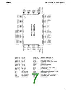
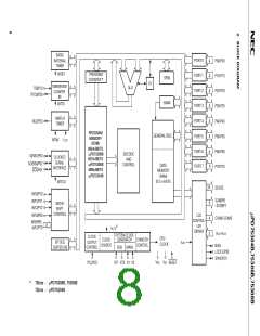
µPD75304B,75306B,75308B
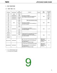
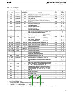
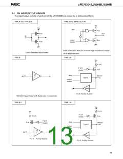
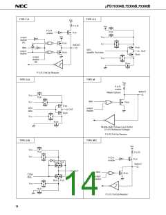
3.2 NON-PORT PINS
Dual-
Function Pin
I/O Circuit
Type *1
After
Reset
Input/Output
Pin Name
Function
Input
P13
P20
P22
B - C
E - B
E - B
TI0
PTO0
PCL
External event pulse input pin to timer/event counter
Timer/event counter output pin
Clock output pin
Input
Input
Input
Input/output
Input/output
Fixed frequency output pin (for buzzer or system clock
trimming)
E - B
F - A
F - B
Input
Input
Input
P23
P01
BUZ
SCK
Input/output
Input/output
Serial clock input/output pin
Serial data output pin
Serial bus input/output pin
P02
P03
SO/SB0
SI/SB1
Input/output
Input/output
Serial data input pin
Serial bus input/output pin
Input
Input
M - C
B
Edge detection vectored interrupt input pin (both rising
edge and falling edge detection effective)
P00
P10
INT4
Input
Clock synchronous
system
Edge detection vectored
interrupt input pin (detection
INT0
INT1
Input
Input
Input
Input
B - C
B - C
edge selectable)
Asynchronous
P11
P12
Edge detection testable input
pin (rising edge detection)
INT2
Asynchronous
Input/output
Input/output
Output
P60 to P63
P70 to P73
—
F - A
F - A
G - A
G - C
G - B
KR0 to KR3
KR4 to KR7
S0 to S23
Parallel falling edge detection testable input pin
Parallel falling edge detection testable input pin
Segment signal output pin
Input
Input
*2
Output
BP0 to BP7
—
S24 to S31
Segment signal output pin
*2
Output
COM0 to COM3
Common signal output pin
*2
LCD drive power supply pin
On-chip split resistor (mask option)
VLC0 to VLC2
—
—
—
—
Output
—
—
BIAS
External split resistor cut output pin
*3
Input/output
P30
E - B
LCDCL *4
External expansion driver drive clock output pin
Input
External expansion driver synchronization clock output
pin
P31
—
Input/output
Input
Input
—
E - B
—
SYNC *4
Main system clock oscillation crystal/ceramic connection
pin. For external clock, the external clock signal is input
to X1 and its opposite phase is input to X2.
X1, X2
Subsystem clock oscillation crystal connection pin. For
external clock, the external clock signal is input to XT1
and XT2 is opened. XT1 can be used as a 1-bit input
(test) pin.
XT1
XT2
Input
—
—
—
—
—
B
System reset input pin
NO CONNECTION
—
—
—
—
RESET
Input
—
—
—
NC *5
—
—
—
VDD
VSS
—
—
—
—
Positive power supply pin
GND potential pin
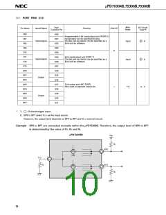
*
1.
: Schmitt trigger input
2. Display outputs are selected with VLCX shown below as the input source.
S0 to S31: VLC1, COM0 to COM2: VLC2, COM3: VLC0
However, the level of each display output depends on the display output and VLCX external circuit.
11

 NEC [ NEC ]