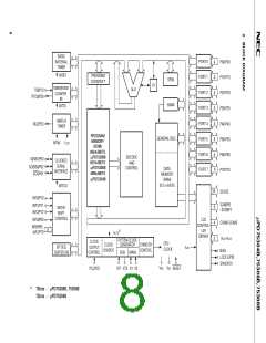
µPD75304B,75306B,75308B
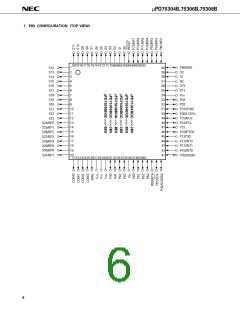
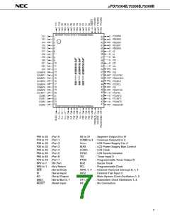
80 79 78 77 76 75 74 73 72 71 70 69 68 67 66 65
P70/KR4
P63/KR3
S12
S13
1
2
64
63
S14
S15
S16
S17
S18
P62/KR2
P61/KR1
P60/KR0
X2
3
62
4
5
6
7
61
60
59
58
X1
µ
µ
µ
S19
S20
S21
S22
NC
XT2
XT1
8
9
57
56
55
54
53
52
51
50
49
48
47
46
45
10
11
12
13
14
15
16
17
18
19
20
VDD
S23
P33
P32
S24/BP0
S25/BP1
S26/BP2
S27/BP3
S28/BP4
S29/BP5
S30/BP6
S31/BP7
COM0
P31/SYNC
P30/LCDCL
P23/BUZ
P22/PCL
P21
P20/PTO0
P13/TI0
P12/INT2
P11/INT1
21
22
23
24
44
43
42
41
COM1
COM2
COM3
P10/INT0
P03/SI/SB1
25 26 27 28 29 30 31 32 33 34 35 36 37 38 39 40
P00 to 03 : Port 0
P10 to 13 : Port 1
P20 to 23 : Port 2
P30 to 33 : Port 3
P40 to 43 : Port 4
P50 to 53 : Port 5
P60 to 63 : Port 6
P70 to 73 : Port 7
S0 to 31
: Segment Output 0 to 31
COM0 to 3 : Common Output 0 to 3
VLC0-2
BIAS
LCDCL
SYNC
TI0
PTO0
BUZ
PCL
INT0, 1, 4
INT2
X1, 2
XT1, 2
NC
: LCD Power Supply 0 to 2
: LCD Power Supply Bias Control
: LCD Clock
: LCD Synchronization
: Timer Input 0
: Programmable Timer Output 0
: Buzzer Clock
: Programmable Clock
: External Vectored Interrupt 0, 1, 4
: External Test Input 2
: Main System Clock Oscillation 1, 2
: Subsystem Clock Oscillation 1, 2
: No Connection
BP0 to 7
KR0 to 7
SCK
: Bit Port
: Key Return
: Serial Clock
: Serial Input
: Serial Output
: Serial Bus 0, 1
: Reset Input
SI
SO
SB0,1
RESET
7

 NEC [ NEC ]