µPD75216A
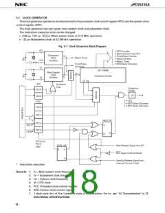
5.2 CLOCK GENERATOR
The clock generator operations are determined by the processor clock control register (PCC) and the system clock
control register (SCC).
The clock generator has two types: main system clock and subsystem clock.
The instruction execution time can be changed.
•
•
0.95 µs, 1.91 µs, 15.3 µs (Main system clock: at 4.19 MHz operation)
122 µs (Subsystem clock: at 32.768 kHz operation)
Fig. 5-1 Clock Generator Block Diagram
XT1
• FIP Controller
• Basic Interval Timer (BT)
• Timer/Event Counter
• Serial Interface
• Watch Timer
• INT0 Noise Eliminator
Subsystem
Clock
Oscillator
f
XT
Watch Timer
XT2
X1
Timer/Pulse
Generator
1/8~1/4096
Main System
Clock
Oscillator
f
XX
Frequency Divider
f
X
X2
1/2 1/6
SCC
Oscillation
Stop
Frequency
Divider
SCC3
1/4
Φ
SCC0
PCC
• CPU
• INT0 Noise Eliminator
• INT1 Noise Eliminator
PCC0
PCC1
4
HALT F/F
S
PCC2
PCC3
HALT*
STOP*
Q
R
PCC2 and
PCC3
Clear
Wait Release Signal from BT
RES Signal (Internal Reset)
STOP F/F
Q
S
R
Standby Release Signal from
Interrupt Control Circuit
*
Instruction execution
Remarks 1. fX = Main system clock frequency
2. fXT = Subsystem clock frequency
3. fXX = System clock frequency
4. Φ = CPU clock
5. PCC: Processor clock control register
6. SCC: System clock control register
7. 1 clock cycle (tCY) of Φ is 1 machine cycle of an instruction. For tCY, see ”AC Characteristics“ in 12.
ELECTRICAL SPECIFICATIONS.
18

 NEC [ NEC ]