CHAPTER 3 CPU FUNCTIONS
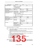
Peripheral Function
Register Name
WDTM1
Access
k
Watchdog timer 1 (WDT1)
Write
2 to 4
<Calculation of number of waits>
{(1/fx) × 2/((2 + m)/fCPU)} + 1
fx: Oscillation frequency
Watchdog timer 2 (WDT2)
WDTM2
Write
3 (fixed)
1 (fixed)
16-bit timer/event counters 00 to 05
(TM00 to TM05)Note 1
TMC00 to TMC05
Read-modify-write
A wait occurs during write
Clocked serial interfaces 0 and 1 with CSIA0B0 to CSIA0BF,
WriteNote 2 (when performing
continuous write)
0 to 18
automatic transmit/receive function
(CSIA0, CSIA1)Note 3
CSIA1B0 to CSIA1BF
<Calculation of number of waits>
{(1/fSCKA) × 5 – (4 + m)/fCPU)}/{((2 + m)/fCPU)}
However, 1 wait if fCPU = fxx if the CKSAn1 and CKSAn0 bits of the CSISn register
are 0.
fSCKA: CSIA selection clock frequency
I2C0Note 4, I2C1Note 5
IICS0, IICS1
Read
Read
1 (fixed)
1 (fixed)
Asynchronous serial interfaces 0 to 2
(UART0 to UART2)Note 6
ASIS0 to ASIS2
Real-time output functions 0 and 1
(RTO0, RTO1)Note 7
RTBL0, RTBL1,
RTBH0, RTBH1
Write
1
(when bits RTPOE0 and
RTPOE1 of RTPC0 and
RTPC1 registers = 0)
A/D converter
ADM, ADS, PFM, PFT
ADCR, ADCRH
Write
Read
1 to 5
1 to 5
<Calculation of maximum number of waits>
{(1/fAD) × 2/(2 + m)/fCPU } + 1
fAD: A/D selection clock frequency
Number of waits to be added = (2 + m) × k [clocks]
Notes 1. TM02 and TM03 are available only in the V850ES/KG1 and V850ES/KJ1; TM04 and TM05 are
available only in the V850ES/KJ1.
2. If fetched from the on-chip RAM, the number of waits is as shown above.
If fetched from the external memory, the number of waits may be fewer than the number shown
above.
The effect of the external memory access cycle differs depending on the wait settings, etc.
However, the number of waits above is the maximum value.
3. CSIA1 is available only in the V850ES/KG1 and V850ES/KJ1.
4. I2C0 is available only in the products with I2C.
5. I2C1 is available only in the V850ES/KJ1 (µPD703216Y, 703217Y, and 70F3217Y).
6. UART2 is available only in the V850ES/KJ1.
7. RTO1 is available only in the V850ES/KJ1.
Caution When the CPU operates on the subclock and no clock is input to the X1 pin, do not access a
register in which a wait occurs using an access method that causes a wait. If a wait occurs,
it can only be released by a reset.
User’s Manual U15862EJ3V0UD
135

 NEC [ NEC ]