CHAPTER 3 CPU FUNCTIONS
3.4.8 Cautions
Be sure to set the following register before using the V850ES/KF1, V850ES/KG1 and V850ES/KJ1.
•
System wait control register (VSWC)
After setting the VSWC register, set the other registers as required.
When using an external bus, set the VSWC register and then set the various pins to the control mode by setting
the port-related registers.
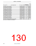
(1) System wait control register (VSWC)
The system wait control register (VSWC) controls the bus access wait time for the on-chip peripheral I/O
registers.
Access to the on-chip peripheral I/O register lasts 3 clocks (during no wait), but in the V850ES/KF1,
V850ES/KG1 and V850ES/KJ1, waits are required according to the operation frequency. Set the values shown
below to the VSWC register according to the operation frequency that is used.
This register can be read or written in 8-bit units (Address: FFFFF06EH, After reset: 77H).
Operation Conditions
REGC = VDD = 5 V 10%,
Operation Frequency (fCLK)
8 MHz ≤ fCLK < 16.6 MHz
16.6 MHz ≤ fCLK ≤ 20 MHz
2 MHz ≤ fCLK < 8.3 MHz
8.3 MHz ≤ fCLK ≤ 16 MHz
fCLK ≤ 16 MHz
VSWC Setting
00H
In PLL mode (OSC = 2 to 5 MHz)
01H
00H
01H
00H
REGC = Capacity, VDD = 4.0 to 5.5 V
REGC = VDD = 2.7 to 4.0 V
Other than above
(REGC = VDD = 4.0 to 5.5 V)
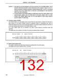
(2) Access to special on-chip peripheral I/O register
This product has two types of internal system buses.
One type is for the CPU bus and the other is for the peripheral bus to interface with low-speed peripheral
hardware.
Since the CPU bus clock and peripheral bus clock are asynchronous, if a conflict occurs during access
between the CPU and peripheral hardware, illegal data may be passed unexpectedly. Therefore, when
accessing peripheral hardware that may cause a conflict, the number of access cycles is changed so that the
data is received/passed correctly in the CPU. As a result, the CPU does not shift to the next instruction
processing and enters the wait status. When this wait status occurs, the number of execution clocks of the
instruction is increased by the number of wait clocks.
Note this with caution when performing real-time processing.
When accessing a special on-chip peripheral I/O register, additional waits may be required further to the waits
set by the VSWC register.
The access conditions at that time and the method to calculate the number of waits to be inserted (number of
CPU clocks) are shown below.
User’s Manual U15862EJ3V0UD
134

 NEC [ NEC ]