µPD6121, 6122
3.2 Standard versions with Ver II specs. (µPD6121-002, 6122-002)
*
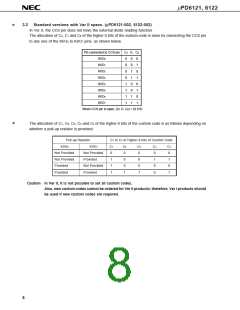
In Ver II, the CCS pin does not have the external diode reading function.
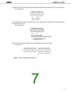
The allocation of C2, C1 and C0 of the higher 8 bits of the custom code is done by connecting the CCS pin
to any one of the KI/O0 to KI/O7 pins, as shown below.
Pin connected to CCS pin
C2
C
1
C
0
KI/O
KI/O
KI/O
KI/O
KI/O
KI/O
KI/O
KI/O
0
1
2
3
4
5
6
7
0
0
0
0
1
1
1
1
C
0
0
1
1
0
0
1
1
0
1
0
1
0
1
0
1
When CCS pin is open, (C
2
C1
0
) = (0 0 0)
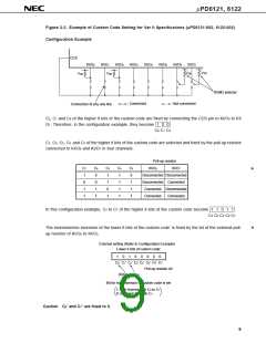
The allocation of C7, C6, C5, C4 and C3 of the higher 8 bits of the custom code is as follows depending on
whether a pull-up resistor is provided.
*
Pull-up Resistor
C7 to C3 of Higher 8 bits of Custom Code
KI/O6
KI/O7
C7
0
C6
0
C5
0
C4
0
C3
0
Not Provided
Not Provided
Provided
Not Provided
Provided
1
0
0
1
1
Not Provided
1
0
0
0
0
Provided
Provided
1
1
1
0
1
Caution In Ver II, it is not possible to set all custom codes.
Also, new custom codes cannot be ordered for Ver II products; therefore, Ver I products should
be used if new custom codes are required.
8

 NEC [ NEC ]