µPD178023, 178024
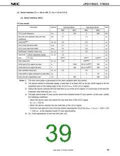
(2) Serial interface (TA = –40 to +85 °C, VDD = 3.5 to 5.5 V)
(a) Serial interface (IIC0)
I2C bus mode
Parameter
Symbol
Standard Mode
High-speed Mode
MIN. MAX.
Unit
MIN.
MAX.
100
–
SCL0 clock frequency
fCLK
tBUF
0
0
400
–
kHz
Bus free time (between stop and start
conditions)
4.7
1.3
µs
Hold timeNote 1
tHD : STA
tLOW
4.0
4.7
4.0
4.7
5.0
0Note 2
250
–
–
–
0.6
–
µs
µs
µs
µs
µs
µs
ns
ns
ns
µs
ns
pF
SCL0 clock low-level width
SCL0 clock high-level width
Start/restart condition setup time
1.3
–
tHIGH
–
0.6
–
tSU : STA
tHD : DAT
–
0.6
–
–
Data hold
time
CBUS compatible master
I2C bus
–
–
–
0Note 2
0.9Note 3
–
Data setup time
tSU : DAT
tR
–
100Note 4
SDA0 and SCL0 signal rise time
SDA0 and SCL0 signal fall time
Stop condition setup time
1000
300
–
20+0.1CbNote 5
300
300
–
tF
–
20+0.1CbNote 5
tSU : STO
4.0
–
0.6
0
Pulse width of spike restrained by input filter tSP
Each bus line capacitative load Cb
–
50
–
400
–
400
Notes 1. The first clock pulse is generated at the start condition after this period.
2. The device needs to internally supply a hold time of at least 300 ns for the SDA0 signal to fill the
undefined area at the falling edge of the SCL0 (VIHmin. of the SCL0 signal).
3. Unless the device extends the low hold time (tLOW) of the SCL0 signal, it is necessary to fill only the
maximum data hold time (tHD : DAT).
4. The high-speed mode I2C bus can be used in the standard mode I2C bus system. In this case, satisfy
the following conditions:
• When the device does not extend the low hold time of the SCL0 signal
tSU : DAT ≥ 250 ns
• When the device extends the low hold time of the SCL0 signal
Send the next data bit to the SDA line before releasing the SCL0 line (tRmax. + tSU:DAT = 1000 + 250
= 1250 ns : in the standard mode I2C bus specification)
5. Cb: Total capacitance of one bus line (unit: pF)
Data Sheet U14126EJ1V0DS00
39

 NEC [ NEC ]