µPD178023, 178024
8. ELECTRICAL SPECIFICATIONS
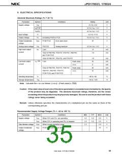
Absolute Maximum Ratings (TA = 25 °C)
Parameter
Symbol
VDD
Conditions
Rating
Unit
V
Supply voltage
–0.3 to +6.0
–0.3 to VDD + 0.3
–0.3 to VDD + 0.3
–0.3 to +11.0
–0.3 to VDD + 0.3
16
VDDPORT
VDDPLL
VI
V
V
Input voltage
V
Output voltage
VO
Excluding P130 to P132
V
Output breakdown
voltage
VBDS
P130-P132
N-ch open drain
V
Analog input voltage
VAN
IOH
P10-P15
1 pin
Analog input pin
–0.3 to VDD + 0.3
V
High-level output
current
–8
mA
mA
Total of P00-P06, P30-P37, P54-P57, P60-P67,
and P120-P125
–15
Total of P40-P47, P50-P53, and P70-P77
–15
16
8
mA
mA
mA
mA
mA
Note
Low-level output
current
IOL
1 pin
Peak value
r.m.s
Total of P00-P06, P30-P37, P40-P47, Peak value
30
15
P50-P57, P60-P67, P70-P77,
P120-P125, and P130-P132
r.m.s
Operating temperature
Storage temperature
TA
–40 to +85
°C
°C
Tstg
–55 to +125
Note Calculate the r.m.s as follows: [r.m.s] = [Peak value] x √Duty
Caution If the rated value of even one of the above parameters is exceeded even momentarily, the quality
of the product may be degraded. The absolute maximum ratings, therefore, are the values
exceeding which the product may be physically damaged. Be sure to use the product with these
ratings never being exceeded.
Remark Unless otherwise specified, the characteristics of a multiplexed pin are the same as those of the
corresponding port pin.
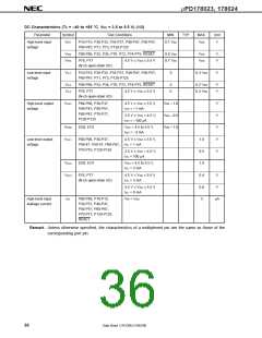
Recommended Supply Voltage Ranges (TA = –40 to +85 °C)
Parameter
Symbol
VDD1
Conditions
When CPU and PLL are operating
When CPU is operating and PLL is stopped
When crystal oscillation stops
MIN.
4.5
TYP.
5.0
MAX.
5.5
Unit
V
Supply voltage
VDD2
3.5
5.0
5.5
V
Data retention voltage
VDDR
VBDS
2.3
5.5
V
Output breakdown
voltage
P130-P132 (N-ch open drain)
15
V
Data Sheet U14126EJ1V0DS00
35

 NEC [ NEC ]