µPD178023, 178024
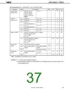
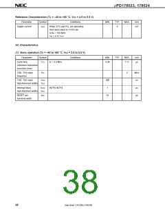
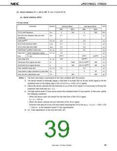
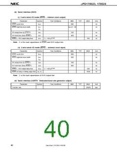
DC Characteristics (TA = –40 to +85 °C, VDD = 3.5 to 5.5 V) (2/2)
Parameter
Symbol
ILIL
Test Conditions
MIN.
TYP.
MAX.
–3
Unit
Low-level input
leakage current
P00-P06, P10-P15,
VIN = 0 V
µA
P30-P37, P40-P47,
P50-P57, P60-P67,
P70-P77, P120-P125,
RESET
Output off
ILOH1
ILOL1
ILOH2
P130-P132
P130-P132
VOUT = 15 V
VOUT = 0 V
VOUT = VDD
–3
3
µA
µA
µA
leakage current
P76, P77
–3
(at N-ch open drain I/O)
ILOL2
P76, P77
VOUT = 0 V
3
µA
(at N-ch open drain I/O)
ILOH3
ILOL3
IDD1
EO0, EO1
EO0, EO1
VOUT = VDD
VOUT = 0 V
–3
3
µA
µA
mA
Supply currentNote
When CPU is operating and PLL is stopped.
Sine wave input to X1 pin
At fX = 4.5 MHz
4.0
20
VIN = VDD
IDD2
In HALT mode with PLL stopped.
Sine wave input to X1 pin
At fX = 4.5 MHz
0.35
0.70
5.5
mA
VIN = VDD
Data retention
voltage
VDDR1
VDDR2
When crystal resonator is oscillating
3.5
2.2
V
V
When crystal oscillation is
stopped
Power-failure detection
function
VDDR3
Data memory retained
2.0
V
Data retention
current
IDDR1
When crystal oscillation is
stopped
TA = 25 °C,
2.0
2.0
4.0
20
µA
VDD = 5 V
IDDR2
µA
Note Excluding AVDD current and VDDPLL current.
Remarks 1. fX: System clock oscillation frequency
2. Unless otherwise specified, the characteristics of a multiplexed pin are the same as those of the
corresponding port pin.
Data Sheet U14126EJ1V0DS00
37

 NEC [ NEC ]