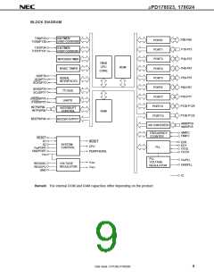
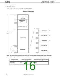
µPD178023, 178024
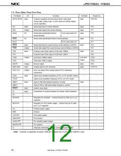
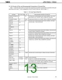
1.3 I/O Circuits of Pins and Recommended Connections of Unused Pins
Table 1-1 shows the types of the I/O circuits of the respective pins and the recommended connections of the pins
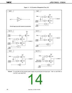
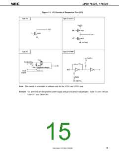
when they are not used. For the configuration of the I/O circuit of each pin, refer to Figure 1-1.
Table 1-1. I/O Circuit Type of Each Pin
Pin Name
P00/INTP0-P04/INTP4
P05, P06
I/O Circuit Type
8
I/O
I/O
Recommended Connection of Unused Pin
Set these pins in general-purpose input mode in software, and connect
each of them to VDD, VDDPORT, GND, or GNDPORT via resistor.
P10/ANI0-P15/ANI5
P30-P32
25
5
Input
I/O
Connect each of them to VDD, VDDPORT, GND, or GNDPORT via resistor.
Set these pins in general-purpose input mode in software, and output
low-level signal. Leave unconnected.
P33/TI50
5-K
P34/TI51
P35
5
P36/BEEP0
P37
P40-P47
5-A
5
Set these pins in general-purpose input mode in software, and connect each
of them to GND or GNDPORT via resistor.
P50-P57
P60-P67
Set these pins in general-purpose input mode in software, and connect each
of them to VDD, VDDPORT, GND, or GNDPORT via resistor.
5
Set these pins in general-purpose input mode in software, and output
low-level signal. Leave unconnected.
P70/SI3
5-K
5
Set these pins in general-purpose input mode in software, and connect each
of them to VDD, VDDPORT, GND, or GNDPORT via resistor.
P71/SO3
P72/SCK3
P73
5-K
5
P74/RXD0
P75/TXD0
P76/SDA0
P77/SCL0
P120-P125
P130/TO50
P131/TO51
P132
5-K
5
10-D
5
19
Output Set these pins to low-level output in software and leave unconnected.
EO0, EO1
VCOL, VCOH
AMIFC, FMIFC
DTS-EO1
DTS-AMP
Output Leave unconnected.
Input
Disable PLL in software and select pull-down.
Set these pins in general-purpose input port mode in software and connect
each of them to VDD, VDDPORT, GND, or GNDPORT via resistor.
REGOSC, REGCPU
–
–
Input
–
Connect these pins to GND via 0.1-µF capacitor.
RESET
VDDPLL
GNDPLL
IC
2
–
Connect this pin to VDD.
–
Directly connect these pins to GND or GNDPORT.
Data Sheet U14126EJ1V0DS00
13

 NEC [ NEC ]