CHAPTER 11 10-BIT A/D CONVERTER (µPD789436 AND 789456 SUBSERIES)
11.3 10-Bit A/D Converter Control Registers
The 10-bit A/D converter is controlled by the following two registers.
•
•
A/D converter mode register 0 (ADM0)
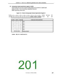
Analog input channel specification register 0 (ADS0)
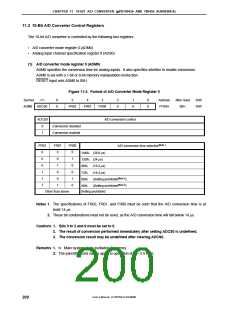
(1) A/D converter mode register 0 (ADM0)
ADM0 specifies the conversion time for analog inputs. It also specifies whether to enable conversion.
ADM0 is set with a 1-bit or 8-bit memory manipulation instruction.
RESET input sets ADM0 to 00H.
Figure 11-2. Format of A/D Converter Mode Register 0
Symbol
ADM0
<7>
6
0
5
4
3
2
0
1
0
0
0
Address
FF80H
After reset
00H
R/W
R/W
ADCS0
FR02
FR01
FR00
ADCS0
A/D conversion control
0
1
Conversion disabled
Conversion enabled
A/D conversion time selectionNote 1
FR02
FR01
FR00
0
0
0
1
1
1
0
0
1
0
0
1
0
1
0
0
1
0
144/fX (28.8 µs)
120/fX (24 µs)
96/fX
72/fX
60/fX
48/fX
(19.2 µs)
(14.4 µs)
(Setting prohibitedNote 2
(Setting prohibitedNote 2
)
)
Other than above
Setting prohibited
Notes 1. The specifications of FR02, FR01, and FR00 must be such that the A/D conversion time is at
least 14 µs.
2. These bit combinations must not be used, as the A/D conversion time will fall below 14 µs.
Cautions 1. Bits 0 to 2 and 6 must be set to 0.
2. The result of conversion performed immediately after setting ADCS0 is undefined.
3. The conversion result may be undefined after clearing ADCS0.
Remarks 1. fX: Main system clock oscillation frequency
2. The parenthesized values apply to operation at fX = 5.0 MHz.
User’s Manual U15075EJ1V0UM00
200

 NEC [ NEC ]