CHAPTER 11 10-BIT A/D CONVERTER (µPD789436 AND 789456 SUBSERIES)
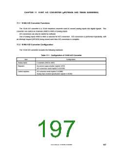
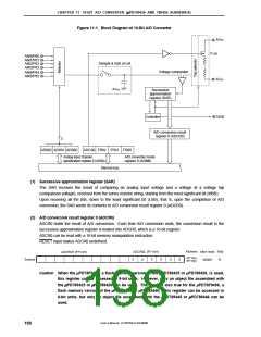
Figure 11-1. Block Diagram of 10-Bit A/D Converter
AVDD
P-ch
ANI0/P60
ANI1/P61
ANI2/P62
ANI3/P63
ANI4/P64
ANI5/P65
Sample & hold circuit
Voltage comparator
AVSS
AVSS
Successive
approximation
register (SAR)
INTAD0
Controller
A/D conversion result
register 0 (ADCR0)
3
ADS02 ADS01 ADS00
ADCS0 FR02 FR01 FR00
Analog input channel
specification register 0 (ADS0)
A/D converter mode
register 0 (ADM0)
Internal bus
(1) Successive approximation register (SAR)
The SAR receives the result of comparing an analog input voltage and a voltage at a voltage tap
(comparison voltage), received from the series resistor string, starting from the most significant bit (MSB).
Upon receiving all the bits, down to the least significant bit (LSB), that is, upon the completion of A/D
conversion, the SAR sends its contents to A/D conversion result register 0 (ADCR0).
(2) A/D conversion result register 0 (ADCR0)
ADCR0 holds the result of A/D conversion. Each time A/D conversion ends, the conversion result in the
successive approximation register is loaded into ADCR0, which is a 10-bit register.
ADCR0 can be read with a 16-bit memory manipulation instruction.
RESET input makes ADCR0 undefined.
Address
After reset R/W
ADCR0L (FF14H)
ADCR0H (FF14H)
FF14H,
FF15H
Symbol
0
0
0
0
0
0
0000H
R
Caution When the µPD78F9436, a flash memory version of the µPD789425 or µPD789426, is used,
this register can be accessed in 8-bit units. However, only an object file assembled with
the µPD789425 or µPD789426 can be used. The same is also true for the µPD78F9456, a
flash memory version of the µPD789445 or µPD789446: This register can be accessed in
8-bit units, but only an object file assembled with the µPD789445 or µPD789446 can be
used.
User’s Manual U15075EJ1V0UM00
198

 NEC [ NEC ]