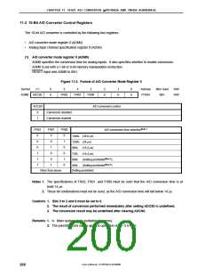
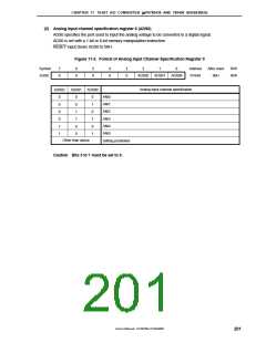
CHAPTER 11 10-BIT A/D CONVERTER (µPD789436 AND 789456 SUBSERIES)
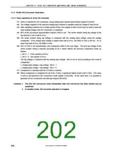
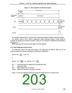
Figure 11-4. Basic Operation of 10-Bit A/D Converter
Conversion time
Sampling
time
A/D converter
operation
Sampling
Undefined
A/D conversion
Conversion
result
SAR
ADCR0
INTAD0
Conversion
result
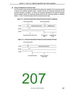
A/D conversion continues until bit 7 (ADCS0) of A/D converter mode register 0 (ADM0) is reset (0) by software.
If an attempt is made to write to ADM0 or analog input channel specification register 0 (ADS0) during A/D
conversion, the ongoing A/D conversion is canceled. In this case, A/D conversion is restarted from the beginning, if
ADCS0 is set (1).
RESET input makes A/D conversion result register 0 (ADCR0) undefined.
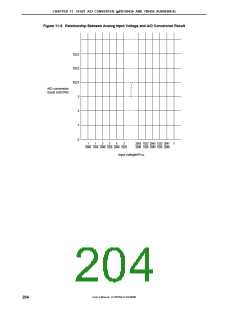
11.4.2 Input voltage and conversion result
The relationships between the analog input voltage at the analog input pins (ANI0 to ANI5) and the A/D
conversion result (A/D conversion result register 0 (ADCR0)) are represented by:
VIN
AVDD
ADCR0 = INT (
or
× 1,024 + 0.5)
AVDD
1,024
AVDD
1,024
(ADCR0 − 0.5) ×
≤ VIN < (ADCR0 + 0.5) ×
INT( ):
VIN:
Function that returns the integer part of a parenthesized value
Analog input voltage
AVDD:
Supply voltage for the A/D converter
ADCR0: Value in A/D conversion result register 0 (ADCR0)
Figure 11-5 shows the relationship between the analog input voltage and the A/D conversion result.
User’s Manual U15075EJ1V0UM00
203

 NEC [ NEC ]