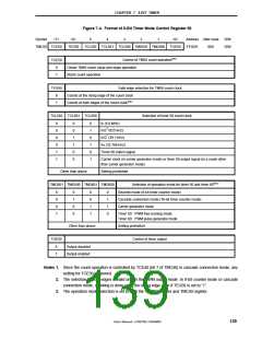
CHAPTER 7 8-BIT TIMER
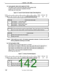
(3) Carrier generator output control register 60 (TCA60)
This register is used to set the timer output data in carrier generator mode.
TCA60 is set with an 8-bit memory manipulation instruction.
RESET input sets TCA60 to 00H.
Figure 7-6. Format of Carrier Generator Output Control Register 60
Symbol
TCA60
7
0
6
0
5
0
4
0
3
0
<2>
<1>
<0>
Address After reset R/W
FF4FH 00H
RMC60 NRZB60 NRZ60
W
RMC60
0
Control of remote control output
When NRZB60 = 1, a carrier pulse is output.
When NRZB60 = 0, a low level is output.
1
When NRZB60 = 1, high-level signal is output.
When NRZB60 = 0, a low level is output.
NRZB60 This is the bit that stores the next data to be output to NRZ60. When a match signal occurs (for a match with
timer 50), the data is output to NRZ60. Input the required value to NRZ60 by program beforehand.
NRZ60
No return zero data
0
1
Outputs low-level signal (carrier clock is stopped)
Outputs carrier pulse
Caution TCA60 cannot be set with a 1-bit memory manipulation instruction. Be sure to use an 8-bit
memory manipulation instruction to set TCA60.
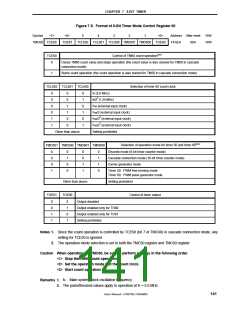
(4) Port mode register 3 (PM3)
This register is used to set the I/O mode of port 3 in 1-bit units.
When using the P31/TO50/INTP1/TMI60 pin as a timer output, set the PM31 and P31 output latch to 0.
When using the P32/TO60/INTP2 pin as a timer output, set the PM32 and P32 output latch to 0.
When using the P33/TO61/INTP3 pin as a timer output, set the PM33 and P33 output latch to 0.
PM3 is set with a 1-bit or 8-bit memory manipulation instruction.
RESET input sets PM3 to FFH.
Figure 7-7. Format of Port Mode Register 3
Symbol
PM3
7
1
6
1
5
1
4
1
3
2
1
0
Address
FF23H
After reset
FFH
R/W
R/W
PM33
PM32
PM31
PM30
PM3n
I/O mode of P3n pin
(n = 0 to 3)
0
1
Output mode (output buffer is ON)
Input mode (output buffer is OFF)
142
User’s Manual U15075EJ1V0UM00

 NEC [ NEC ]