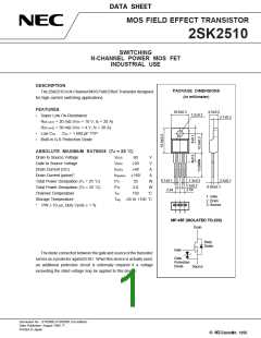
2SK2510
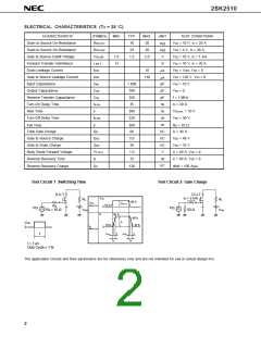
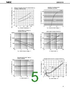
ELECTRICAL CHARACTERISTICS (TA = 25 ˚C)
CHARACTERISTIC
Drain to Source On-Resistance
Drain to Source On-Resistance
Gate to Source Cutoff Voltage
Forward Transfer Admittance
Drain Leakage Current
SYMBOL
RDS (on)1
RDS (on)2
VGS (off)
| yfs |
IDSS
MIN.
TYP.
16
MAX.
20
UNIT
TEST CONDITIONS
VGS = 10 V, ID = 20 A
VGS = 4 V, ID = 20 A
VDS = 10 V, ID = 1 mA
VDS = 10 V, ID = 20 A
VDS = VDSS, VGS = 0
VGS = ±20 V, VDS = 0
VDS = 10 V
mΩ
mΩ
V
24
30
1.0
13
1.5
2.0
S
10
µA
µA
pF
pF
pF
ns
ns
ns
ns
nC
nC
nC
V
Gate to Source Leakage Current
Input Capacitance
IGSS
±10
Ciss
1 600
780
350
35
Output Capacitance
Coss
VGS = 0
Reverse Transfer Capacitance
Turn-On Delay Time
Crss
f = 1 MHz
td (on)
ID = 20 A
Rise Time
tr
380
220
VGS (on) = 10 V
VDD = 30 V
Turn-Off Delay Time
td (off)
Fall Time
tf
300
69
RG = 10 Ω
Total Gate Charge
QG
ID = 40 A
Gate to Source Charge
Gate to Drain Charge
Body Diode Forward Voltage
Reverse Recovery Time
QGS
QGD
VF (S-D)
trr
5.0
26
VDD = 48 V
VGS = 10 V
1.0
72
IF = 40 A, VGS = 0
IF = 40 A, VGS = 0
ns
nC
Reverse Recovery Charge
Qrr
130
di/dt = 100 A/µs
Test Circuit 1 Switching Time
Test Circuit 2 Gate Charge
D.U.T.
D.U.T.
= 2 mA
V
GS
IG
R
L
RL
90 %
V
GS
Wave Form
V
GS (on)
10 %
R
G
0
PG.
PG.
RG
= 10 Ω
50 Ω
VDD
VDD
I
D
90 %
90 %
10 %
I
D
V
0
GS
10 %
I
D
0
Wave Form
t
d (on)
t
r
t
d (off)
t
f
t
t
on
t
off
t = 1 µs
Duty Cycle ≤ 1 %
The application circuits and their parameters are for references only and are not intended for use in actual design-in's.
2

 NEC [ NEC ]