DDR3(L) 4Gb SDRAM
NT5CB(C)512M8DN / NT5CB(C)256M16DP
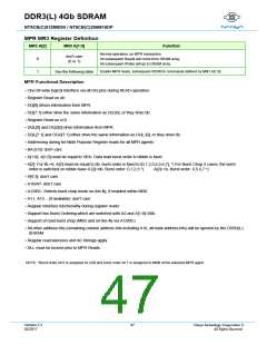
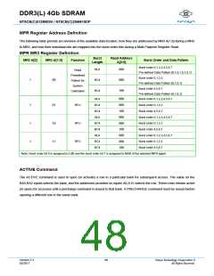
MPR Register Address Definition
The following table provide an overview of the available data location, how they are addressed by MR3 A[1:0] during a MRS
to MR3, and how their individual bits are mapped into the burst order bits during a Multi Purpose Register Read.
MPR MR3 Register Definition
Burst
Length
Read Address
A[2:0]
MR3 A[2]
MR3 A[1:0]
Function
Burst Order and Data Pattern
Burst order 0,1,2,3,4,5,6,7
Pre-defined Data Pattern [0,1,0,1,0,1,0,1]
Burst order 0,1,2,3
BL8
BC4
BC4
000
000
100
Read
Predefined
Pattern for
System
1
00
Pre-defined Data Pattern [0,1,0,1]
Burst order 4,5,6,7
Calibration
Pre-defined Data Pattern [0,1,0,1]
Burst order 0,1,2,3,4,5,6,7
BL8
BC4
BC4
BL8
BC4
BC4
BL8
BC4
BC4
000
000
100
000
000
100
000
000
100
1
1
1
01
10
11
RFU
RFU
RFU
Burst order 0,1,2,3
Burst order 4,5,6,7
Burst order 0,1,2,3,4,5,6,7
Burst order 0,1,2,3
Burst order 4,5,6,7
Burst order 0,1,2,3,4,5,6,7
Burst order 0,1,2,3
Burst order 4,5,6,7
Note: Burst order bit 0 is assigned to LSB and the burst order bit 7 is assigned to MSB of the selected MPR agent.
ACTIVE Command
The ACTIVE command is used to open (or activate) a row in a particular bank for subsequent access. The value on the
BA0-BA2 inputs selects the bank, and the addresses provided on inputs A0-A15 selects the row. These rows remain active
(or open) for accesses until a precharge command is issued to that bank. A PRECHARGE command must be issued before
opening a different row in the same bank.
Version 2.3
02/2017
48
Nanya Technology Cooperation ©
All Rights Reserved.

 NANYA [ Nanya Technology Corporation. ]