DDR3(L) 4Gb SDRAM
NT5CB(C)512M8DN / NT5CB(C)256M16DP
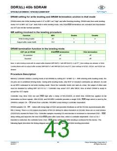
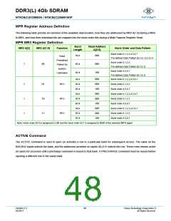
MPR MR3 Register Definition
MR3 A[2]
MR3 A[1:0]
Function
Normal operation, no MPR transaction.
don't care
(0 or 1)
0
1
All subsequent Reads will come from DRAM array.
All subsequent Writes will go to DRAM array.
Enable MPR mode, subsequent RD/RDA commands defined by MR3 A[1:0].
See the following table
MPR Functional Description
• One bit wide logical interface via all DQ pins during READ operation.
• Register Read on x8:
• DQ[0] drives information from MPR.
• DQ[7:1] either drive the same information as DQ [0], or they drive 0b.
• Register Read on x16:
• DQL[0] and DQU[0] drive information from MPR.
• DQL[7:1] and DQU[7:1] either drive the same information as DQL [0], or they drive 0b.
• Addressing during for Multi Purpose Register reads for all MPR agents:
• BA [2:0]: don’t care
• A[1:0]: A[1:0] must be equal to ‘00’b. Data read burst order in nibble is fixed
• A[2]: For BL=8, A[2] must be equal to 0b, burst order is fixed to [0,1,2,3,4,5,6,7], *) For Burst Chop 4 cases, the burst
order is switched on nibble base A [2]=0b, Burst order: 0,1,2,3 *)
A[2]=1b, Burst order: 4,5,6,7 *)
• A[9:3]: don’t care
• A10/AP: don’t care
• A12/BC: Selects burst chop mode on-the-fly, if enabled within MR0.
• A11, A13... (if available): don’t care
• Regular interface functionality during register reads:
• Support two Burst Ordering which are switched with A2 and A[1:0]=00b.
• Support of read burst chop (MRS and on-the-fly via A12/BC)
• All other address bits (remaining column address bits including A10, all bank address bits) will be ignored by the DDR3(L)
SDRAM.
• Regular read latencies and AC timings apply.
• DLL must be locked prior to MPR Reads.
NOTE: *Burst order bit 0 is assigned to LSB and burst order bit 7 is assigned to MSB of the selected MPR agent.
Version 2.3
02/2017
47
Nanya Technology Cooperation ©
All Rights Reserved.

 NANYA [ Nanya Technology Corporation. ]