DDR3(L) 4Gb SDRAM
NT5CB(C)512M8DN / NT5CB(C)256M16DP
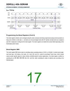
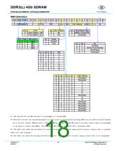
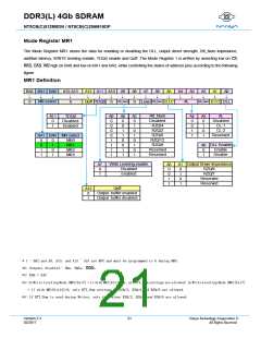
MR0 Definition
BA2 BA1 BA0
A15-A13
A12 A11 A10 A9
A8
A7
A6
A5
A4
A3
A2
A1
A0
↓
↓
↓
↓
↓
↓
↓
↓
↓
↓
↓
↓
↓
↓
↓
↓
↓
MR select
WR
CAS Latency
BL
0
0
PPD
DLL TM
RBT CL
PPD
Slow exit(DLL off)
Fast exit(DLL on)
DLL Reset
No
Read Burst Type
Nibble Sequential
Interleave
A12
0
1
A8
0
1
A3
0
1
Yes
mode
Normal
Test
BA1 BA0 MR select
A7
0
1
0
0
1
1
0
1
0
1
MR0
MR1
MR2
MR3
BL
8(Fixed)
A1
0
A0
0
BC4 or 8 (on the fly)
BC4(Fixed)
0
1
1
0
WR
16
5
6
7
Reserved
A11 A10 A9
1
1
0
0
0
0
1
1
1
1
0
0
1
1
0
0
1
1
0
1
0
1
0
1
0
1
8
10
12
14
CAS Latency
Reserved
Reserved
A6
0
0
0
0
1
1
1
1
0
0
0
0
1
1
1
1
A5
0
0
1
1
0
0
1
1
0
0
1
1
0
0
1
1
A4
0
1
0
1
0
1
0
1
0
1
0
1
0
1
0
1
A2
0
0
0
0
0
0
0
0
1
1
1
1
1
1
1
1
6
7
8
9
10
11
Reserved
13
14
Reserved
Reserved
Reserved
Reserved
Reserved
*1: BA2 and A13~A15 are RFU and must be programmed to 0 during MRS.
*2: WR (write recovery for autoprecharge)min in clock cycles is calculated by dividing tWR(in ns) by tCK(in ns) and rounding
up to the next integer: WRmin[cycles] = Roundup(tWR[ns] / tCK[ns]). The WR value in the mode register must be programmed
to be equal or larger than WRmin. The programmed WR value is used with tRP to determine tDAL.
*3: The table only shows the encodings for a given Cas Latency. For actual supported Cas Latency, please refer to speedbin
tables for each frequency
*4: The table only shows the encodings for Write Recovery. For actual Write recovery timing, please refer to AC timingtable.
Version 2.3
02/2017
18
Nanya Technology Cooperation ©
All Rights Reserved.

 NANYA [ Nanya Technology Corporation. ]