DDR3(L) 4Gb SDRAM
NT5CB(C)512M8DN / NT5CB(C)256M16DP
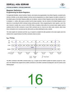
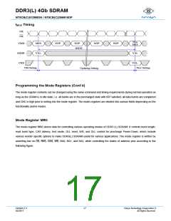
tMOD Timing
CK
CK
Non
MRS
CMD
ADDR
CKE
MRS
VAL
NOP
NOP
NOP
NOP
tMOD
VAL
VAL
Old Setting
New Setting
Updating Setting
Programming the Mode Registers (Cont’d)
The mode register contents can be changed using the same command and timing requirements during normal operation as
long as the DRAM is in idle state, i.e. all banks are in the precharged state with tRP satisfied, all data bursts are completed
and CKE is high prior to writing into the mode register. The mode registers are divided into various fields depending on the
functionality and/or modes.
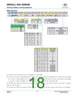
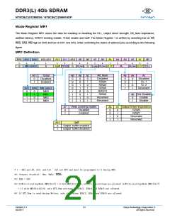
Mode Register MR0
The mode-register MR0 stores data for controlling various operating modes of DDR3 (L) SDRAM. It controls burst length,
read burst type, CAS latency, test mode, DLL reset, WR, and DLL control for precharge Power-Down, which include
various vendor specific options to make DDR3(L) SDRAM useful for various applications. The mode register is written by
asserting low on , RA, A, WE, BA0, BA1, and BA2, while controlling the states of address pins according to the
following figure.
Version 2.3
02/2017
17
Nanya Technology Cooperation ©
All Rights Reserved.

 NANYA [ Nanya Technology Corporation. ]