NTC Proprietary
Level: Property
DDR3(L)-2Gb SDRAM
NT5CB(C)256M8JQ/NT5CB(C)128M16JR
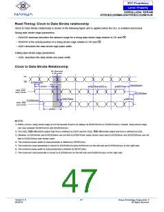
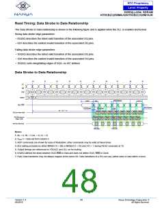
Read Timing; Data Strobe to Data Relationship
The Data Strobe to Data relationship is shown in the following figure and is applied when the DLL is enabled and locked.
Rising data strobe edge parameters:
• tDQSQ describes the latest valid transition of the associated DQ pins.
• tQH describes the earliest invalid transition of the associated DQ pins.
Falling data strobe edge parameters:
• tDQSQ describes the latest valid transition of the associated DQ pins.
• tQH describes the earliest invalid transition of the associated DQ pins.
• tDQSQ; both rising/falling edges of DQS, no tAC defined
Data Strobe to Data Relationship
T0
T1
T2
T3
T4
T5
T6
T7
T8
T9
CK
CK
CMD
READ
NOP
NOP
NOP
NOP
NOP
NOP
NOP
NOP
NOP
Bank
Col n
Address
DQS, DQS
tDQSQmax
tRPRE
tQH
tRPST
tHZ(DQ)min
tLZ(DQ)min
tDQSQmin
tQH
RL = AL + CL
Dout
n
Dout
n +1
Dout
n +2
Dout
n +3
Dout
n +4
Dout
n +5
Dout
n +6
Dout
n +7
DQ (Last data valid)
DQ (First data no
longer valid)
Dout
n
Dout
n +1
Dout
n +2
Dout
n +3
Dout
n +4
Dout
n +5
Dout
n +6
Dout
n +7
All DQ collectively
Valid data
Valid data
Notes:
1. BL = 8, RL = 5 (AL = 0, CL = 5)
2. DOUT n = data-out from column n.
3. NOP commands are shown for ease of illustration; other commands may be valid at these times.
4. BL8 setting activated by either MR0[A1:0 = 00] or MR0[A1:0 = 01] and A12 = 1 during READ command at T0.
5. Output timings are referenced to VDDQ/2, and DLL on for locking.
6. tDQSQ defines the skew between DQS, to Data and does not define DQS, to Clock.
7. Early Data transitions may not always happen at the same DQ. Data transitions of a DQ can vary (either early or late) within a burst.
Version 1.4
05/2019
48
Nanya Technology Cooperation ©
All Rights Reserved.

 NANYA [ Nanya Technology Corporation. ]