• This PDF catalog is downloaded from the website of Murata Manufacturing co., ltd. Therefore, it’s specifications are subject to change or our products in it may be discontinued without advance notice. Please check with our
• Please read rating and !CAUTION (for storage, operating, rating, soldering, mounting and handling) in this catalog to prevent smoking and/or burning, etc.
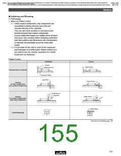
!Note
!Note
C02E.pdf
sales representatives or product engineers before ordering.
• This catalog has only typical specifications because there is no space for detailed specifications. Therefore, please approve our product specifications or transact the approval sheet for product specifications before ordering0. 9.9.18
• This PDF catalog has only typical specifications because there is no space for detailed specifications. Therefore, please approve our product specifications or transact the approval sheet for product specifications before ordering.
!Caution
!Caution
Continued from the preceding page.
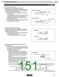
6. Electrical Test on Printed Circuit Board
1. Confirm position of the support pin or specific jig, when
inspecting the electrical performance of a capacitor after
mounting on the printed circuit board.
[Not Recommended]
Peeling
1-1. Avoid bending printed circuit board by the pressure
of a test pin, etc.
Test-pin
The thrusting force of the test probe can flex the PCB,
resulting in cracked chips or open solder joints.
Provide support pins on the back side of the PCB to
prevent warping or flexing.
[Recommended]
Support Pin
1-2. Avoid vibration of the board by shock when a test pin
contacts a printed circuit board.
Test-pin
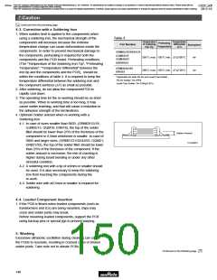
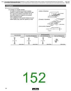
7. Printed Circuit Board Cropping
1. After mounting a capacitor on a printed circuit board, do
not apply any stress to the capacitor that is caused by
bending or twisting the board.
8
[Bending]
[Twisting]
1-1. In cropping the board, the stress as shown right may
cause the capacitor to crack.
Try not to apply this type of stress to a capacitor.
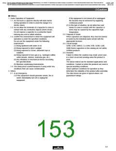
2. Check of the cropping method for the printed circuit
board in advance.
2-1. Printed circuit board cropping shall be carried out by
using a jig or an apparatus to prevent the mechanical
stress which can occur to the board.
(1) Example of a suitable jig
Recommended example: the board should be
pushed as close to the near the cropping jig as
possible and from the back side of board in order
to minimize the compressive stress applied to
capacitor.
[Outline of Jig]
Printed Circuit Board
V-groove
Not recommended example* when the board is
pushed at a point far from the cropping jig and
from the front side of board as below, the
capacitor may form a crack caused by the tensile
stress applied to capacitor.
Boad Cropping Jig
Recommended
Not recommended
Direction of Load
Direction of Load
Load Point
Printed Circuit Board
Components
Components
Load Point
Printed Circuit Board
Continued on the following page.
149

 MURATA [ muRata ]