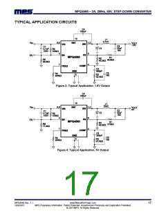
MPQ4560 – 2A, 2MHz, 55V STEP-DOWN CONVERTER
The system may have another significant zero if
the output capacitor has a large capacitance or a
high ESR value. This zero is located at:
values, set the compensation zero (fZ1) <0.25 ×fC
to provide sufficient phase margin. C3 is then:
4
C3
1
2πR3 fC
fESR
2πC2RESR
3. C5 is required if the ESR zero of the output
capacitor is located at <0.5 ×fSW , or the following
relationship is valid:
In this case, a third pole set by the compensation
capacitor (C5) and the compensation resistor can
compensate for the effect of the ESR zero. This
pole is located at:
fS
2
1
2πC2RESR
1
fP3
If this is the case, use C5 to set the pole (fP3) at
the location of the ESR zero. Determine the C5:
2πC5R3
The goal of compensation design is to shape the
converter transfer function for a desired loop
gain. The system crossover frequency where the
feedback loop has unity gain is important: Lower
crossover frequencies result in slower line and
load transient responses, while higher crossover
frequencies lead to system instability. Generally,
set the crossover frequency to ~0.1×fSW.
C2RESR
C5
R3
High-Frequency Operation
The switching frequency of MPQ4560 can be
programmed up to 2MHz by an external resistor.
The minimum on time of MPQ4560 is about
100ns (typ). Pulse-skipping occurs more readily
at higher switching frequencies due to the
minimum ON time.
Table 3: Compensation Values for Typical
Output Voltage/Capacitor Combinations
VOUT
(V)
C2
(µF)
R3
(kΩ)
C3
(pF)
C6
(pF)
L (µH)
4.7
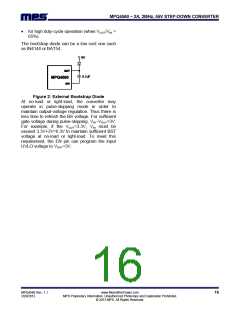
Since the internal bootstrap circuitry has higher
impedance, which may not sufficiently charge the
bootstrap capacitor during each (1−D)×τS
charging period, add an external bootstrap
charging diode if the switching frequency is about
2MHz (see External Bootstrap Diode section for
detailed implementation information).
1.8
2.5
3.3
5
33
22
22
33
22
32.4
26.1
68.1
47.5
16
680
680
220
330
470
None
None
None
None
2
4.7 - 6.8
6.8 -10
15 - 22
10
With higher switching frequencies, the capacitors’
inductive reactances (XL) dominate so that the
ESL of input/output capacitors determine the
input/output ripple voltages at higher switching
frequencies. As a result, use high-frequency
ceramic capacitors as input decoupling
capacitors and output filtering capacitors for high-
frequency operation.
12
To optimize the compensation components for
conditions not listed in Table 3, follow these
steps:
1. Choose R3 to set the desired crossover
frequency:
External Bootstrap Diode
An external bootstrap diode from the 5V rail to
the BST pin may enhance the efficiency under
the following conditions:
2πC2 f VOUT
R3
C
GEAGCS
VFB
There is a 5V rail available in the system;
VIN ≤5V;
Where fC is the desired crossover frequency.
2. Choose C3 to achieve the desired phase
margin. For applications with typical inductor
3.3V<VOUT<5V; and
MPQ4560 Rev. 1.1
3/29/2013
www.MonolithicPower.com
MPS Proprietary Information. Unauthorized Photocopy and Duplication Prohibited.
© 2013 MPS. All Rights Reserved.
15

 MPS [ MONOLITHIC POWER SYSTEMS ]