MPQ4560 – 2A, 2MHz, 55V STEP-DOWN CONVERTER
~5V. When the voltage between the BST and SW
During a short circuit, the VFB voltage is low and
pulls down VSS to ~100mV above VFB. Removing
the short circuit causes the output voltage to
recover with VSS. When VFB is high enough, the
frequency and current limit return to normal
values.
nodes is less than its regulation, a PMOS pass
transistor from VIN to BST turns ON. The
charging current path is from VIN, BST and then
to SW. An external circuit must provide enough
voltage headroom to facilitate charging.
As long as VIN is sufficiently higher than VSW, the
bootstrap capacitor can charge. When the power
MOSFET is ON, VIN≈VSW so the bootstrap
capacitor cannot charge. When the external
diode is ON, the difference between VIN and VSW
is at its largest, thus making it the best period to
charge. When there is no current in the inductor,
VSW=VOUT so the difference between VIN and VOUT
can charge the bootstrap capacitor.
Startup and Shutdown
If both VIN and VEN exceed their respective
thresholds, the chip starts. The reference block
initiates to generate a stable reference voltage
and currents, and then the internal regulator is
enabled. The regulator provides a stable supply
for the remaining circuitries.
While the internal supply rail is up, an internal
timer holds the power MOSFET OFF for about
50µs to blank the startup noise. When the
internal soft-start block is enabled, it first holds its
SS output low to ensure the remaining circuitries
are ready and then slowly ramps up.
At higher duty cycles, the time period available
for bootstrap charging is shorter so the bootstrap
capacitor may not sufficiently charge. If the
internal circuit does not have sufficient voltage
and the bootstrap capacitor is not charged, extra
external circuitry can ensure the bootstrap
voltage is within the normal operational region.
Three events can shut down the chip: VEN LOW,
VIN LOW and thermal shutdown. During
shutdown, the power MOSFET turns OFF first to
avoid any fault triggering. Then VCOMP and the
internal supply rail drop.
The DC quiescent current of the floating driver is
about 20µA. Make sure the bleeding current at
the SW node exceeds this value, such that:
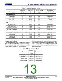
Programmable Oscillator
VO
An external resistor (RFREQ) from the FREQ pin to
ground sets the MPQ4560 oscillating frequency.
The value of RFREQ can be calculated from:
IO
20A
(R1 R2)
Current Comparator and Current Limit
100000
A current-sense MOSFET accurately senses the
power MOSFET’s current. The result goes to the
high-speed current comparator for current-mode
control.: When the power MOSFET turns ON, the
comparator is first blanked till the end of the turn-
on transition to avoid noise issues. The
comparator then compares the power switch
current to VCOMP. When the sensed current
exceeds VCOMP, the comparator output is LOW,
turning OFF the power MOSFET. The
cycle-by-cycle maximum current of the internal
power MOSFET is internally limited.
RFREQ(kΩ) =
-5
fS(kHz)
For example, for fSW=500kHz, RFREQ=195kΩ.
Short Circuit Protection
When the output is shorted to the ground, the
switching frequency folds back and the current
limit falls to lower the short-circuit current. When
VFB is zero, the current limit drops to about 50%
of its full current limit. When VFB exceeds 0.4V,
current limit reaches 100%.
MPQ4560 Rev. 1.1
3/29/2013
www.MonolithicPower.com
MPS Proprietary Information. Unauthorized Photocopy and Duplication Prohibited.
© 2013 MPS. All Rights Reserved.
11

 MPS [ MONOLITHIC POWER SYSTEMS ]