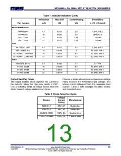
MPQ4560 – 2A, 2MHz, 55V, STEP-DOWN CONVERTER
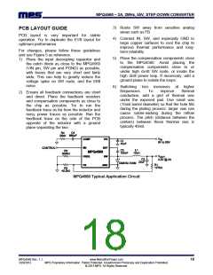
3) Route SW away from sensitive analog
areas such as FB.
PCB LAYOUT GUIDE
PCB layout is very important for stable
operation. Try to duplicate the EVB layout for
optimum performance.
4) Connect IN, SW, and especially GND to
large copper surfaces to cool the chip to
improve thermal performance and long-
term reliability.
For changes, please follow these guidelines
and use Figure 5 as reference.
5) Place the compensation components close
to the MPQ4560. Avoid placing the
compensation components close to or
under high dv/dt SW node, or inside the
high di/dt power loop. If necessary, add a
ground plane to isolate the loops.
1) Place the input decoupling capacitor and
the catch diode as close to the MPQ4560
(VIN pin, SW pin and PGND) as possible,
with traces that are very short and fairly
wide. This can help to greatly reduce the
voltage spike on SW node, and the EMI
noise.
6) Switching loss increases at higher
frequencies.
To
improve
thermal
2) Ensure all feedback connections are short
and direct. Place the feedback resistors
and compensation components as close to
the chip as possible. Try to run the
feedback trace as far from the inductor and
noisy power traces as possible. Run the
feedback trace on the side of the PCB
opposite of the inductor with a ground
plane separating the two.
conduction, add a grid of thermal vias
under the exposed pad. Use small vias
(15mil barrel diameter) so that the hole fills
during the plating process: larger vias can
cause solder-wicking during the reflow
process. The pitch (distance between the
centers) between these thermal vias is
typically 40mil.
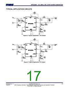
MPQ4560 Typical Application Circuit
MPQ4560 Rev. 1.1
3/29/2013
www.MonolithicPower.com
MPS Proprietary Information. Patent Protected. Unauthorized Photocopy and Duplication Prohibited.
© 2013 MPS. All Rights Reserved.
18

 MPS [ MONOLITHIC POWER SYSTEMS ]