MPQ4559 – 1.5A, 2MHz, 55V STEP-DOWN CONVERTER AEC-Q100 QUALIFIED
With higher switching frequencies, the inductive
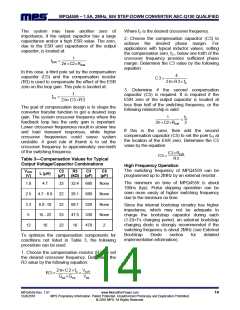
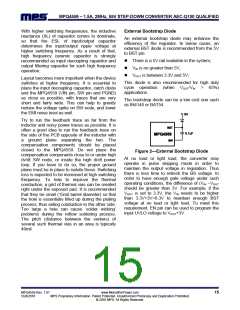
External Bootstrap Diode
reactance (XL) of capacitor comes to dominate,
so that the ESL of input/output capacitor
determines the input/output ripple voltage at
higher switching frequency. As a result of that,
high frequency ceramic capacitor is strongly
recommended as input decoupling capacitor and
output filtering capacitor for such high frequency
operation.
An external bootstrap diode may enhance the
efficiency of the regulator. In below cases, an
external BST diode is recommended from the 5V
to BST pin:
There is a 5V rail available in the system;
VIN is no greater than 5V;
VOUT is between 3.3V and 5V;
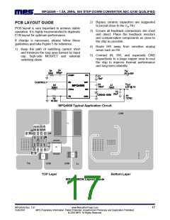
Layout becomes more important when the device
switches at higher frequency. It is essential to
place the input decoupling capacitor, catch diode
and the MPQ4559 (VIN pin, SW pin and PGND)
as close as possible, with traces that are very
short and fairly wide. This can help to greatly
reduce the voltage spike on SW node, and lower
the EMI noise level as well.
This diode is also recommended for high duty
cycle operation (when VOUT/VIN
applications.
>
65%)
The bootstrap diode can be a low cost one such
as IN4148 or BAT54.
Try to run the feedback trace as far from the
inductor and noisy power traces as possible. It is
often a good idea to run the feedback trace on
the side of the PCB opposite of the inductor with
a ground plane separating the two. The
compensation components should be placed
closed to the MPQ4559. Do not place the
compensation components close to or under high
dv/dt SW node, or inside the high di/dt power
loop. If you have to do so, the proper ground
plane must be in place to isolate those. Switching
loss is expected to be increased at high switching
frequency. To help to improve the thermal
conduction, a grid of thermal vias can be created
right under the exposed pad. It is recommended
that they be small (15mil barrel diameter) so that
the hole is essentially filled up during the plating
process, thus aiding conduction to the other side.
Too large a hole can cause ‘solder wicking’
problems during the reflow soldering process.
The pitch (distance between the centers) of
several such thermal vias in an area is typically
40mil.
Figure 2—External Bootstrap Diode
At no load or light load, the converter may
operate in pulse skipping mode in order to
maintain the output voltage in regulation. Thus
there is less time to refresh the BS voltage. In
order to have enough gate voltage under such
operating conditions, the difference of (VIN –VOUT
should be greater than 3V. For example, if the
VOUT is set to 3.3V, the VIN needs to be higher
than 3.3V+3V=6.3V to maintain enough BST
voltage at no load or light load. To meet this
requirement, EN pin can be used to program the
input UVLO voltage to VOUT+3V.
MPQ4559 Rev. 1.01
5/24/2016
www.MonolithicPower.com
MPS Proprietary Information. Patent Protected. Unauthorized Photocopy and Duplication Prohibited.
© 2016 MPS. All Rights Reserved.
15

 MPS [ MONOLITHIC POWER SYSTEMS ]