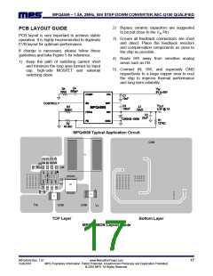
MPQ4559 – 1.5A, 2MHz, 55V STEP-DOWN CONVERTER AEC-Q100 QUALIFIED
Input Capacitor
VOUT
VOUT
ΔVOUT
1
RESR
The input current to the step-down converter is
discontinuous, therefore a capacitor is required to
supply the AC current to the step-down converter
while maintaining the DC input voltage. Use low
ESR capacitors for the best performance.
Ceramic capacitors are preferred, but tantalum or
low-ESR electrolytic capacitors may also suffice.
fS L
VIN
The characteristics of the output capacitor also
affect the stability of the regulation system. The
MPQ4559 can be optimized for a wide range of
capacitance and ESR values.
Compensation Components
MPQ4559 employs current mode control for easy
compensation and fast transient response. The
system stability and transient response are
controlled through the COMP pin. COMP pin is
the output of the internal error amplifier. A series
capacitor-resistor combination sets a pole-zero
combination to control the characteristics of the
control system. The DC gain of the voltage
feedback loop is given by:
For simplification, choose the input capacitor with
RMS current rating greater than half of the
maximum load current. The input capacitor (C1)
can be electrolytic, tantalum or ceramic.
When using electrolytic or tantalum capacitors, a
small, high quality ceramic capacitor, i.e. 0.1μF,
should be placed as close to the IC as possible.
When using ceramic capacitors, make sure that
they have enough capacitance to provide
sufficient charge to prevent excessive voltage
ripple at input. The input voltage ripple caused by
capacitance can be estimated by:
VFB
AVDC RLOAD GCS AVEA
VOUT
Where AVEA is the error amplifier voltage gain,
400V/V; GCS is the current sense
transconductance, 5.6A/V; RLOAD is the load
resistor value.
ILOAD
VOUT
VOUT
VIN
1
fS C1
VIN
V
IN
Output Capacitor
The system has two poles of importance. One is
due to the compensation capacitor (C3), the
output resistor of error amplifier. The other is due
to the output capacitor and the load resistor.
These poles are located at:
The output capacitor (C2) is required to maintain
the DC output voltage. Ceramic, tantalum, or low
ESR electrolytic capacitors are recommended.
Low ESR capacitors are preferred to keep the
output voltage ripple low. The output voltage
ripple can be estimated by:
GEA
fP1
2πC3 AVEA
VOUT
VOUT
VIN
1
RESR
VOUT
1
fS L
8 fS C2
1
fP2
2πC2RLOAD
Where L is the inductor value and RESR is the
equivalent series resistance (ESR) value of the
output capacitor.
Where,
GEA
is
the
error
amplifier
transconductance, 120μA/V.
In the case of ceramic capacitors, the impedance
at the switching frequency is dominated by the
capacitance. The output voltage ripple is mainly
caused by the capacitance. For simplification, the
output voltage ripple can be estimated by:
The system has one zero of importance, due to
the compensation capacitor (C3) and the
compensation resistor (R3). This zero is located
at:
1
fZ1
VOUT
8 fS2 L C2
VOUT
2πC3R3
ΔVOUT
1
V
IN
In the case of tantalum or electrolytic capacitors,
the ESR dominates the impedance at the
switching frequency. For simplification, the output
ripple can be approximated to:
MPQ4559 Rev. 1.01
5/24/2016
www.MonolithicPower.com
MPS Proprietary Information. Patent Protected. Unauthorized Photocopy and Duplication Prohibited.
© 2016 MPS. All Rights Reserved.
13

 MPS [ MONOLITHIC POWER SYSTEMS ]