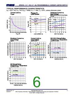
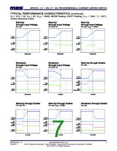
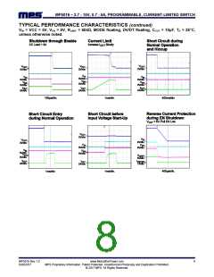
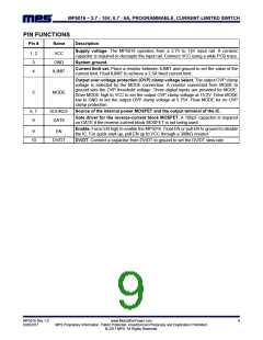
MP5016 – 2.7 - 15V, 0.7 - 5A, PROGRAMMABLE, CURRENT-LIMITED SWITCH
ABSOLUTE MAXIMUM RATINGS (1)
VCC, SOURCE.............................. -0.3V to 26V
MODE............................................ -0.3V to 26V
GATE....................................... SOURCE+ 5.5V
All other pins............................... -0.3V to +5.5V
Junction temperature...............-40°C to +150°C
Lead temperature ....................................260°C
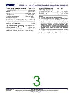
Thermal Resistance
θJA
θJC
QFN-10 (1.5mmx2mm)
(4)
EV5016H-QH-00A ............ 56.......18 ... °C/W
(5)
JESD51-7 ........................ 130......25 ... °C/W
NOTES:
1) Exceeding these ratings may damage the device.
2) The maximum allowable power dissipation is a function of the
maximum junction temperature TJ (MAX), the junction-to-
ambient thermal resistance θJA, and the ambient temperature
TA. The maximum allowable continuous power dissipation at
any ambient temperature is calculated by PD (MAX) = (TJ
(MAX)-TA)/θJA. Exceeding the maximum allowable power
dissipation produces the excessive die temperature, causing
the regulator to go into thermal shutdown. Internal thermal
shutdown circuitry protects the device from permanent
damage.
(2)
Continuous power dissipation (TA = +25°C)
....................................................................................... (4)
QFN-10 (1.5mmx2mm)............................2.23W
Recommended Operating Conditions (3)
Supply voltage (VCC) ..................... 2.7V to 15V
Output voltage (SOURCE).............. 2.7V to 15V
Operating junction temp. (TJ) ...-40°C to +125°C
3) The device is not guaranteed to function outside of its operating
conditions.
4) Measured on EV5016-QH-00A, 2-layer PCB, 50mmx50mm.
5) Measured on JESD51-7, 4-layer PCB.
MP5016 Rev.1.0
6/20/2017
www.MonolithicPower.com
MPS Proprietary Information. Patent Protected. Unauthorized Photocopy and Duplication Prohibited.
© 2017 MPS. All Rights Reserved.
3

 MPS [ MONOLITHIC POWER SYSTEMS ]