MP5016 – 2.7 - 15V, 0.7 - 5A, PROGRAMMABLE, CURRENT-LIMITED SWITCH
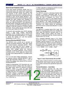
Table 4: K1 Factor Value at External DV/DT
Capacitor
MODE Connection
VCC
C4
C3
R2
K1
5.75
15.2
27
VCC
SOURCE
Low
High
Float
7
6
1
2
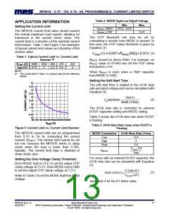
C2
C1
Vclamp
RMODE
Top Layer
7μ*RMODE
R1
For example, when the external DV/DT cap is
47nF and RMODE = 76.8kΩ, the dV/dt slew rate is
1V/ms.
GND
GND
Bottom Layer
VCC
Large Output Capacitor
Figure 4: Recommended Layout
With large output capacitor, if the charge current
during soft start triggers the current limit, the
MP5016 enters hiccup when the current limit is
triggered for 2ms. To avoid start-up failure with a
large output capacitor, a proper dV/dt slew rate
must be set during the soft start to avoid
triggering the current limit.
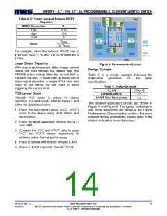
Design Example
Table 5 is a design example following the
application
guidelines
for
the
given
specifications.
Table 5: Design Example
VIN (V)
2.7 to 15
PCB Layout Guide
Current Limit (A)
DV/DT Slew Rate (V/ms)
3.5
3.8
Efficient PCB layout is critical for stable
operation. For best results, refer to Figure 4 and
follow the guidelines below.
The detailed application circuits are shown in
Figure 5 and Figure 6. The typical performance
and circuit waveforms are shown in the Typical
Performance Characteristics section. For more
detailed device applications, please refer to the
related evaluation board datasheet.
1. Place the high-current paths (VCC, VOUT)
close to the device using short, direct, and
wide traces.
2. Place the input capacitors close to the VCC
and GND.
3. Connect the VCC and VOUT pads to large
VCC and VOUT planes respectively to
achieve better thermal performance.
4. Place a current-limit resistor close to ILIMIT.
5. Place a DV/DT capacitor close to DV/DT.
MP5016 Rev.1.0
6/20/2017
www.MonolithicPower.com
MPS Proprietary Information. Patent Protected. Unauthorized Photocopy and Duplication Prohibited.
© 2017 MPS. All Rights Reserved.
14

 MPS [ MONOLITHIC POWER SYSTEMS ]