MP4558 – 1A, 2MHz, 55V STEP-DOWN CONVERTER
This diode is also recommended for high-duty–
place the input decoupling capacitor and the
catch diode as close to the MP4558 (VIN pin, SW
pin and PGND) as close as possible with short
and wide traces. This can help to greatly reduce
the voltage spikes on the SW node, and lower
the EMI noise level.
cycle operation (when VOUT/VIN
applications.
>
65%)
The bootstrap diode can be a low-cost one such
as IN4148 or BAT54.
Route the feedback trace as far from the inductor
and noisy power traces as possible. If possible,
run the feedback trace on the opposite side of
the PCB opposite from the inductor with a ground
plane separating the two. Placing the
compensation components close to the MP4558.
Avoid placing the compensation components
close to or under the high-dv/dt SW node, or
inside the high-di/dt power loop. If this is not
possible, route a ground plane to isolate the
circuit. Switching loss is expected to increase at
high switching frequencies.
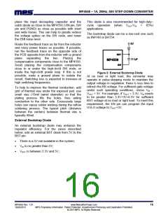
Figure 2: External Bootstrap Diode
At no load or light load, the converter may
operate in pulse-skipping mode to maintain the
output voltage in regulation: there is less time to
refresh the BS voltage. For sufficient gate voltage
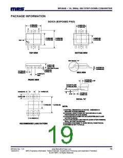
To help to improve the thermal conduction, add
grid of thermal vias under the exposed pad. use
small vias (15mil barrel diameter) so that the
plating process fills the holes, thus aiding
conduction to the other side. Excessively large
holes can cause solder wicking during the reflow
soldering process. The typical pitch (distance
between the centers) between thermal vias is
typically 40mil.
under such operating conditions, chose VIN
–
VOUT > 3V. For example, if VOUT = 3.3V, VIN needs
to be greater than 3.3V+3V=6.3V for sufficient
BST voltage at no load or light load. To meet this
requirement, the EN pin can program the input
UVLO voltage to VOUT+3V.
External Bootstrap Diode
An external bootstrap diode may enhance the
regulator efficiency. For the cases described
below, add an external BST diode from 5V to the
BST pin:
There is a 5V rail available in the system;
VIN is no greater than 5V;
VOUT is between 3.3V and 5V;
MP4558 Rev. 1.01
10/28/2013
www.MonolithicPower.com
MPS Proprietary Information. Patent Protected. Unauthorized Photocopy and Duplication Prohibited.
© 2013 MPS. All Rights Reserved.
16

 MPS [ MONOLITHIC POWER SYSTEMS ]