MP4558 – 1A, 2MHz, 55V STEP-DOWN CONVERTER
The system may have another important zero if
the output capacitor has a large capacitance or a
high ESR value. The zero, due to the ESR and
the output capacitor value, is located at:
2. Choose C3 to achieve the desired phase
margin. For applications with typical inductor
values, set the compensation zero—fZ1—below ¼
the crossover frequency to provide sufficient
phase margin. Determine C3 from the following
equation:
1
fESR
2πC2RESR
4
C3
In this case, a third pole set by the compensation
capacitor (C5) and R3 compensates for the effect
of the ESR zero on the loop gain. This pole is
located at:
2πR3 fC
3. Determine if C5 is required—if the ESR zero of
the output capacitor is located at less than 1/2 fS,
or if the following relationship is valid:
1
fP3
2πC5R3
fS
2
1
The compensation network shapes the converter
transfer function for a desired loop gain. The
feedback-loop unity gain at the system crossover
frequency is important: Lower crossover
frequencies result in slower line and load
transient responses, while higher crossover
frequencies can destabilize the system.
Generally, set the crossover frequency to
approximately 1/10 of the switching frequency.
2πC2RESR
If this is the case, then add C5 to set the pole fP3
at the location of the ESR zero. Determine the
C5 value by the equation:
C2RESR
C5
R3
High-Frequency Operation
The MP4558 switching frequency can be
programmed up to 2MHz by an external resistor.
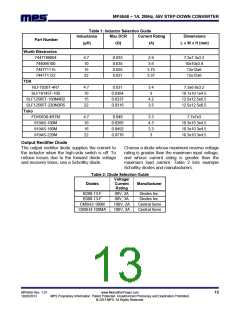
Table 3: Compensation Values for Typical Output
Voltage/Capacitor Combinations
VOUT
(V)
C2
(µF)
R3
(kΩ)
C3
(pF)
C6
(pF)
The minimum MP4558 ON-time is typically about
100ns. Pulse-skipping operation can be seen
more easily at higher switching frequencies due
to the minimum ON-time.
L (µH)
1.8
2.5
3.3
5
4.7
33
22
22
33
22
32.4
26.1
68.1
47.5
16
680
680
220
330
470
None
None
None
None
2
4.7 - 6.8
6.8 -10
15 - 22
10
Since the internal bootstrap circuitry has higher
impedance that may not be adequate to charge
the
bootstrap
capacitor
during
each
(1-D)×tS charging period, add an external
bootstrap charging diode if the switching
frequency is about 2MHz (see External Bootstrap
Diode section for detailed implementation
information).
12
To optimize the compensation components for
conditions not listed in Table 3, use the following
procedure.
With higher switching frequencies, the inductive
reactance (XL) of the capacitor dominates so that
the ESL of the input/output capacitor determines
the input/output ripple voltage at higher switching
frequencies. Because of this ripple, use high-
frequency ceramic capacitors for the input
decoupling capacitor and output the filtering
capacitor for high-frequency operation.
1. Choose R3 to set the desired crossover
frequency. Determine the R3 value from the
following equation:
2πC2 f VOUT
R3
C
GEAGCS
VFB
Layout becomes more important when the device
switches at higher frequencies. For best results,
Where fC is the desired crossover frequency.
MP4558 Rev. 1.01
10/28/2013
www.MonolithicPower.com
MPS Proprietary Information. Patent Protected. Unauthorized Photocopy and Duplication Prohibited.
© 2013 MPS. All Rights Reserved.
15

 MPS [ MONOLITHIC POWER SYSTEMS ]